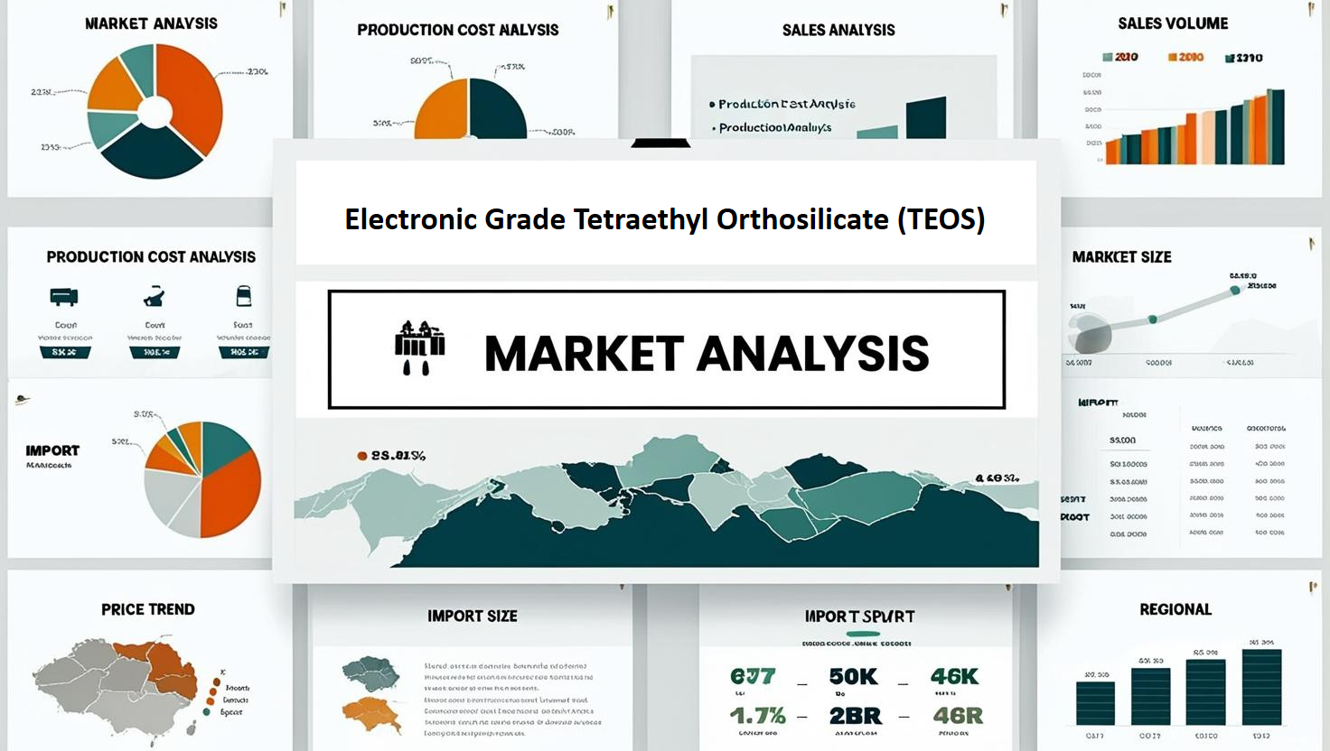
How Electronic Grade Tetraethyl Orthosilicate (TEOS) Became the Invisible Infrastructure Layer Behind Advanced Semiconductor Manufacturing
How Electronic Grade Tetraethyl Orthosilicate (TEOS) Became the Invisible Infrastructure Layer Behind Advanced Semiconductor Manufacturing
Modern semiconductor manufacturing is often described through visible milestones: smaller nodes, faster processors, denser memory, and more powerful AI accelerators. Yet beneath every transistor scaling achievement lies a less visible material infrastructure. One of the most critical among them is Electronic Grade Tetraethyl Orthosilicate (TEOS) market, a precursor chemical that quietly enables the formation of high-quality silicon dioxide films across semiconductor production lines.
The story of Electronic Grade Tetraethyl Orthosilicate (TEOS) is not merely a chemical story. It is an infrastructure story. Every advanced fabrication facility costing between USD 10 billion and USD 30 billion depends on deposition ecosystems where material purity is measured in parts per billion and process consistency is measured in fractions of a nanometer. In such environments, Electronic Grade Tetraethyl Orthosilicate (TEOS) serves as a foundational building block for dielectric layer formation.
A modern wafer may undergo more than 1,000 process steps before completion. Roughly 15%–25% of those steps involve deposition, insulation, or layer engineering activities where oxide quality directly affects device performance. This is where Electronic Grade Tetraethyl Orthosilicate (TEOS) becomes strategically important. A deviation of even 1% in film uniformity can influence yield rates across tens of thousands of wafers annually.
The infrastructure supporting Electronic Grade Tetraethyl Orthosilicate (TEOS) is equally remarkable. Semiconductor-grade chemical manufacturing facilities typically operate with purity thresholds exceeding 99.999%. Storage environments are maintained under tightly controlled temperature and contamination conditions, while transport systems utilize specialized containers designed to prevent moisture intrusion. A single advanced fabrication facility may consume hundreds of tons of process chemicals annually, making logistics reliability as important as material purity.
One of the most significant use cases for Electronic Grade Tetraethyl Orthosilicate (TEOS) is chemical vapor deposition. During deposition, TEOS-based processes create silicon dioxide films that act as insulating barriers between conductive structures. In advanced logic manufacturing, oxide thickness control may require tolerances below 2 nanometers. Such precision explains why manufacturers invest heavily in process monitoring systems capable of generating millions of data points per production day.
The adoption of Electronic Grade Tetraethyl Orthosilicate (TEOS) has accelerated alongside three major technology themes: artificial intelligence infrastructure, memory expansion, and automotive electronics. AI data centers increasingly require high-performance processors containing tens of billions of transistors. Each additional transistor layer introduces greater complexity in insulation architecture, indirectly increasing demand for deposition materials that deliver repeatable oxide quality.
According to Staticker, the Electronic Grade Tetraethyl Orthosilicate (TEOS) market in 2026 is expected to demonstrate sustained expansion, supported by rising semiconductor fabrication investments, advanced packaging deployment, and continued growth in memory and logic production capacity. The market's forecast trajectory remains closely linked to wafer fabrication expansion programs across Asia-Pacific, North America, and Europe, with long-term growth expected to outpace several conventional electronic chemical segments as next-generation device architectures require increasingly sophisticated dielectric deposition processes.
The manufacturing ecosystem surrounding Electronic Grade Tetraethyl Orthosilicate (TEOS) reveals how semiconductor supply chains are evolving. Ten years ago, many fabrication facilities prioritized capacity expansion. Today, yield optimization has become equally important. A 1% yield improvement in a high-volume fab can translate into millions of dollars in annual value creation. Consequently, chemical purity, deposition consistency, and contamination control have become boardroom-level priorities.
Another compelling use case for Electronic Grade Tetraethyl Orthosilicate (TEOS) emerges in advanced memory production. Modern memory devices contain highly complex three-dimensional structures. Certain NAND architectures now exceed 200 layers, creating unprecedented deposition challenges. As layer counts increase, uniform oxide formation becomes more difficult. TEOS-derived films help maintain structural integrity throughout these vertically stacked architectures.
The infrastructure investment behind this trend is substantial. Industry-wide semiconductor capital expenditure has repeatedly crossed tens of billions of dollars annually in recent years. Approximately 20%–30% of fab investments are often directed toward process equipment categories involved in deposition, etching, and thin-film engineering. Since Electronic Grade Tetraethyl Orthosilicate (TEOS) directly supports these process ecosystems, its relevance rises alongside every new fabrication expansion announcement.
Automotive electronics provide another powerful growth narrative. A modern electric vehicle may contain more than 3,000 semiconductor devices distributed across battery management systems, sensors, infotainment platforms, power electronics, and safety modules. Reliability expectations frequently exceed ten years of operational life. Such durability requirements place significant emphasis on dielectric integrity, further reinforcing the role of Electronic Grade Tetraethyl Orthosilicate (TEOS) in semiconductor manufacturing chains serving automotive markets.
Beyond semiconductors, Electronic Grade Tetraethyl Orthosilicate (TEOS) contributes to specialty electronic components where thin-film precision is essential. High-frequency communication systems, advanced sensors, and certain photonic applications increasingly rely on engineered oxide layers. As 5G and future communication standards expand, component density and performance requirements continue to intensify, increasing the importance of deposition chemistry.
From a technical standpoint, the appeal of Electronic Grade Tetraethyl Orthosilicate (TEOS) stems from its ability to produce highly conformal films with excellent process repeatability. Manufacturers frequently evaluate deposition performance through metrics such as step coverage, film stress, dielectric strength, and defect density. Improvements of only a few percentage points in these parameters can significantly influence overall production efficiency.
A useful way to understand the significance of Electronic Grade Tetraethyl Orthosilicate (TEOS) is to compare it with transportation infrastructure. Highways are rarely noticed when functioning properly, yet entire economies depend upon them. Similarly, TEOS is rarely visible in finished electronic products, but processors, memory chips, automotive electronics, and AI accelerators depend upon the oxide layers it helps create. As transistor density continues increasing and fabrication complexity grows, this invisible infrastructure becomes even more critical.
The next phase of the story is likely to be defined by regional semiconductor self-sufficiency initiatives. Governments across major economies have announced multibillion-dollar programs supporting domestic semiconductor manufacturing. Every new fabrication facility adds demand for deposition materials, process chemicals, purification systems, and contamination-control infrastructure. Within that broader ecosystem, Electronic Grade Tetraethyl Orthosilicate (TEOS) remains one of the enabling materials quietly supporting the industry's most ambitious technological advances.
Request for customization: https://staticker.com/reports/electronic-grade-tetraethyl-orthosilicate-teos-market/
Categorias
Leia mais
Cats are playful, curious, and naturally driven to scratch. This instinct is essential for their physical health, mental stimulation, and claw maintenance. For cat owners, providing a dedicated scratching outlet is key to protecting furniture and keeping their pets happy. Two popular solutions that combine function, durability, and style are the sisal scratching post and the modern cat...
Forgetting your login details can be frustrating, especially when you need quick access to your account. If you’ve lost your Lotus365 ID or are having trouble signing in, don’t worry—recovering your account is usually a simple process. This guide will walk you through how to recover your Lotus365 ID and regain access to your Lotus365 login smoothly. Common Reasons for...

Insta Hard: Does This Male Enhancement Supplement Actually Work? ⇨ UPTO 50% OFF 📞📞 https://alltopsupplement.com/Order-Insta-Hard What is Insta Hard? Insta Hard is a dietary supplement designed to address the root causes of erectile dysfunction (ED) and low libido. Unlike prescription medications that act as temporary "band-aids," Insta Hard claims to use a blend of herbal ingredients to support...

Automotive Tire Industry Insights: Straits Research recently introduced the latest update on the Automotive Tire Market that provides an extensive outlook of the market, analyzing key growth opportunities, challenges, risk factors, and emerging trends across diverse geographic regions. The report offers a definitive and meticulous analysis of the Automotive Tire industry size,...
Market Overview According To The Research Report, The Global Federated Learning Market Was Valued At Usd 110.82 Million In 2021 And Is Expected To Reach Usd 266.77 Million By 2030, To Grow At A Cagr Of 10.7% During The Forecast Period. Market Summary The Federated Learning Market is witnessing substantial growth due to increasing data privacy concerns, the rising adoption of artificial...