How Semiconductor Manufacturing Equipment Is Quietly Becoming the World's Most Strategic Industrial Infrastructure
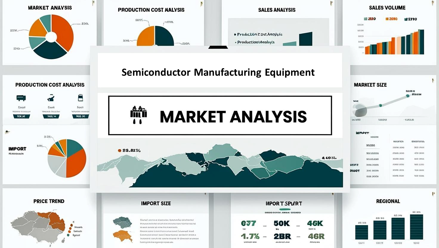
How Semiconductor Manufacturing Equipment Is Quietly Becoming the World's Most Strategic Industrial Infrastructure
The modern digital economy is often described through software, artificial intelligence, cloud computing, and connected devices. Yet beneath every algorithm, data center, electric vehicle, smartphone, and industrial robot sits an invisible layer of physical infrastructure: Semiconductor Manufacturing Equipment.
A single advanced semiconductor fabrication facility today costs between $15 billion and $35 billion to construct, but the building itself contributes only a fraction of the value. The real productivity engine is the ecosystem of Semiconductor Manufacturing Equipment that transforms silicon wafers into billions of functioning transistors.
The scale is staggering. A leading-edge fab processing 50,000 wafer starts per month may contain more than 1,500 individual pieces of Semiconductor Manufacturing Equipment, operating continuously across lithography, deposition, etching, ion implantation, metrology, cleaning, inspection, packaging, and testing stages.
Each wafer can travel over 1,000 kilometers inside a fabrication plant before completion. During this journey, the wafer may undergo 1,200 to 1,800 process steps, with every step relying on highly specialized Semiconductor Manufacturing Equipment capable of operating with nanometer-level precision.
The significance of this infrastructure becomes clear when viewed through transistor density. In 2010, mainstream chips contained a few hundred million transistors. By 2026, advanced processors routinely exceed 50 billion transistors. Such density growth has been possible only because Semiconductor Manufacturing Equipment has continuously improved process precision, throughput, yield optimization, and defect control.
The Infrastructure Race Behind Every Chip
A semiconductor fab is essentially a city-sized manufacturing ecosystem.
Water consumption often exceeds 10 million gallons per day. Electricity demand can reach 100–300 megawatts, equivalent to powering tens of thousands of homes. Cleanroom environments maintain particle concentrations thousands of times cleaner than hospital operating theaters.
However, these facilities derive their economic value from the concentration of Semiconductor Manufacturing Equipment rather than from real estate or utilities.
For example, a single advanced lithography tool may cost more than $200 million. Etching systems can exceed several million dollars per chamber. Deposition tools frequently process thousands of wafers monthly while maintaining atomic-scale layer consistency.
The infrastructure challenge is no longer simply building fabs. Nations are now competing to secure supply chains for Semiconductor Manufacturing Equipment, recognizing that equipment availability directly determines semiconductor production capacity.
Between 2020 and 2026, governments across North America, Europe, East Asia, and the Middle East announced semiconductor-related incentive programs collectively exceeding $250 billion. A significant portion of these investments ultimately supports deployment of Semiconductor Manufacturing Equipment because fabrication output depends on equipment capacity rather than factory floor area alone.
Mapping the Use Cases: Why Every Digital Industry Depends on Semiconductor Manufacturing Equipment
The impact of Semiconductor Manufacturing Equipment extends far beyond semiconductor companies themselves.
A modern electric vehicle typically contains 1,000 to 3,000 semiconductor devices. Advanced driver assistance systems require sensors, processors, memory modules, and power management chips that all originate from fabrication lines dependent on Semiconductor Manufacturing Equipment.
Data centers represent another major demand driver. A hyperscale cloud facility may deploy hundreds of thousands of processors and accelerators. As AI workloads increase, chip complexity rises accordingly, creating greater demand for advanced Semiconductor Manufacturing Equipment capable of supporting smaller process nodes and advanced packaging technologies.
Consumer electronics provide another quantifiable example. Global smartphone shipments remain near the billion-unit level annually. Even modest increases in processor complexity translate into billions of additional transistors requiring fabrication capacity enabled by Semiconductor Manufacturing Equipment.
Industrial automation adds a further layer. Factory robots, machine vision systems, programmable logic controllers, and edge AI devices all depend on semiconductor components manufactured using sophisticated equipment ecosystems.
The result is a multiplier effect. Every dollar invested in Semiconductor Manufacturing Equipment supports downstream economic activity across automotive, healthcare, telecommunications, aerospace, defense, industrial automation, and consumer technology sectors.
Semiconductor Manufacturing Equipment Market Size and Future Capacity Expansion
According to Staticker, the Semiconductor Manufacturing Equipment market in 2026 is positioned around a high-growth phase driven by AI processors, advanced memory expansion, automotive semiconductor demand, and national fabrication investments. Staticker projects continued strong expansion through the forecast period to 2032 as leading-edge logic production, advanced packaging capacity, and power semiconductor manufacturing create sustained capital expenditure cycles. Growth is expected to be supported by increasing wafer fabrication complexity, higher equipment intensity per fab, and rising investments in domestic semiconductor ecosystems across major manufacturing regions.
The Precision Economy: Measuring Success in Nanometers
The economics of Semiconductor Manufacturing Equipment differ from traditional manufacturing industries.
In automotive manufacturing, tolerances are often measured in millimeters. Aerospace production may require micron-level precision. Semiconductor fabrication operates at nanometer scales.
A nanometer represents one-billionth of a meter.
At advanced process nodes, variations of only a few atoms can influence device performance. Consequently, modern Semiconductor Manufacturing Equipment integrates optics, lasers, vacuum systems, plasma physics, materials science, robotics, artificial intelligence, and advanced sensing technologies into a single production environment.
Yield improvement illustrates the financial impact.
Consider a fab producing 50,000 wafers monthly. A yield improvement from 92% to 95% may translate into hundreds of millions of dollars in annual output gains. Because of this relationship, manufacturers continuously invest in upgraded Semiconductor Manufacturing Equipment that improves process consistency and defect detection.
Inspection systems now capture terabytes of production data daily. Machine learning algorithms identify defect patterns before they affect large production batches. This convergence of AI and Semiconductor Manufacturing Equipment is becoming one of the most important themes in semiconductor economics.
Advanced Packaging Is Creating a New Equipment Supercycle
For decades, transistor scaling drove semiconductor progress. Today, advanced packaging is becoming equally important.
Instead of relying solely on smaller transistors, manufacturers increasingly combine multiple chips into highly integrated packages.
This shift is creating entirely new demand categories for Semiconductor Manufacturing Equipment.
High-bandwidth memory integration, chiplet architectures, heterogeneous computing platforms, and AI accelerators require sophisticated bonding, inspection, packaging, and testing systems.
Industry estimates indicate that advanced packaging investment growth is outpacing traditional backend expansion. Some advanced AI packages contain multiple interconnected dies, increasing assembly complexity several-fold compared with conventional chip designs.
As a result, Semiconductor Manufacturing Equipment is evolving beyond wafer fabrication into a broader infrastructure platform supporting complete semiconductor system integration.
The strategic implication is significant. Future semiconductor leadership may depend not only on transistor scaling but also on packaging innovation, making equipment capabilities a central competitive differentiator for manufacturers worldwide.
Request for customization: https://staticker.com/reports/semiconductor-manufacturing-equipment-market/
Categorie
Leggi tutto
" According to the latest report published by Data Bridge Market Research, the Cathode Ray Tube Display Market The global cathode ray tube display market size was valued at USD 885.80 million in 2024 and is projected to reach USD 1488.16 million by 2032, with a CAGR of 6.70% during the forecast period of 2025 to 2032.In this persuasive Cathode Ray Tube Display Market report,...
在當今快速發展的數位娛樂領域,yy game 已成為眾多玩家與業界專業人士關注的焦點,其整合了先進技術與用戶導向設計,提供從休閒小遊戲到競技級應用的完整生態系統;若您希望深入瞭解這個平台的優勢與功能,可以參考 yy game 的詳細介紹,該資源涵蓋了最新的遊戲資訊與安全指南。本文將從技術架構、市場定位、用戶體驗、安全策略及未來趨勢五個面向,全面剖析 YY Game 如何影響現代線上遊戲產業,並為讀者提供一套專業的評估框架。 一、YY Game 的技術架構與核心功能 YY Game 作為一個整合型遊戲平台,其底層技術採用分散式伺服器集群與動態負載均衡機制,確保即使在高併發玩家同時在線的情況下,仍能維持低延遲與高穩定性。平台支援跨裝置同步——包括 Windows、macOS、iOS 及...

" According to the latest report published by Data Bridge Market Research, the Commercial Cleaning Equipment Market CAGR Value Global Commercial Cleaning Equipment Market was valued at USD 2,24,3766 million in 2021 and is expected to reach USD 3,496,049 million by 2029, registering a CAGR of 5.7% during the forecast period of 2022-2029. The market research studies of Commercial...
Sufentanil Market Size, Share, and Growth Forecast : Key Trends and Segment Analysis"Executive Summary: Sufentanil Market Size and Share by Application & Industry The global sufentanil market size was valued at USD 191.66 million in 2024 and is projected to reach USD 395.54 million by 2032, with a CAGR of 10.17% during the forecast period of 2025 to 2032.The leading Sufentanil...
Italy Implements New Digital Age Verification Protocol for Adult Content Starting November 12, Italy will join several other nations in requiring age verification for accessing adult websites online. This move aligns Italy with countries like the United Kingdom, France, and certain U.S. states that have already implemented similar protective measures. The Italian communications authority...