Embedded Hardware Design Company San Jose CA: Scaling Prototypes to Big Production

In Silicon Valley’s hyper-competitive technology theater, speed-to-market and architectural viability are the dividing lines between commercial success and structural failure. For hardware startups and established tech enterprises operating out of San Jose, California, building an early-stage bench prototype that works under perfect laboratory conditions is only the first step. The true engineering hurdle emerges when transitioning that delicate proof-of-concept (PoC) into a high-yielding, mass-manufactured, global Big Production run.
Many hardware teams discover too late that an electronic architecture optimized for rapid local prototyping is fundamentally unsuited for automated, large-scale assembly lines. Component obsolescence, poor board-level thermal management, trace signal corruption, and low manufacturing yields can quickly stall launches and drain engineering capital.
At Jenex Technovation Pvt. Ltd., we have built our global footprint to resolve this exact friction point. As a premium Embedded Hardware Design Company San Jose CA, we don't just sketch schematics; we engineer production-ready physical realities. We build the stable Hardware-Software Bridge required to move custom devices smoothly from Silicon Valley design rooms to mass-production floors across the USA, Canada, Europe, and Australia.
The Silicon Valley Paradox: Why Prototyping Labs Stall at the Factory Gate
San Jose and the broader Bay Area host some of the world's most advanced rapid-prototyping environments. However, a major disconnect persists between localized rapid prototyping and global mass manufacturing. A local lab can easily spin five or ten boards manually, but when automated Surface Mount Technology (SMT) pick-and-place machines must assembly fifty thousand units, tiny layout mistakes turn into expensive disasters.
If component clearances fail to account for automated panel routing blades, ceramic capacitors will micro-crack under stress. If copper balances are uneven across multi-layer stack-ups, boards will warp under intense reflow oven heat.
To prevent these costly failures and ensure 99.9% manufacturing yields, Jenex Technovation Pvt. Ltd. implements a rigorous, seven-pillar Design for Manufacturing (DFM) engineering framework:
1. Supply Chain Resilience and Lifecycle Footprint Scrubbing
In modern electronics design, component availability dictates your engineering timeline. Specifying a specialized chip without verifying its global allocation status can instantly ruin a mass market launch if that component goes End-of-Life (EOL) mid-run.
-
The Jenex Protocol: We evaluate your Bill of Materials (BOM) using real-time supply chain data analytics. For every microcontroller, sensor, and power IC, we implement pin-compatible, drop-in alternative layouts on the physical PCB. This silicon-agnostic footprint design ensures your production line keeps moving even during sudden regional supply shocks.
2. High-Density Interconnect (HDI) and Multi-Layer Signal Integrity
Modern, compact form factors—like edge-computing medical wearables or industrial automation controllers running localized AI/ML Solutions—require advanced, high-density PCB layouts with tight trace tolerances.
-
The Jenex Protocol: We design multi-layer boards using precise blind and buried micro-via structures and controlled-impedance routing geometries. By matching differential pair lengths and isolating sensitive analog lines from noisy power distribution networks, we guarantee absolute Signal Integrity (SI). This strict routing layout ensures your hardware easily sails through strict FCC, CE, and RoHS compliance test chambers on its first pass.
3. Symmetrical Copper Balancing and Advanced Thermal Management
High-performance processors run hot. If a multi-layer board layout lacks strategic thermal pathways, concentrated heat pockets will reduce component life and cause system instability.
-
The Jenex Protocol: We design perfectly balanced multi-layer stack-ups, distributing internal copper planes symmetrically to prevent board warping during liquid reflow soldering. We integrate arrays of thermal micro-vias directly beneath power-hungry silicon elements to pull heat away toward dedicated cooling planes, completely eliminating the need for bulky, heavy external custom heatsinks.
4. Precision Component Normalization for SMT Speed Optimization
Every unique component value or package geometry added to a design forces automated assembly machinery to switch its placement nozzles, slow down its feeding reels, or recalibrate its optical tracking systems.
-
The Jenex Protocol: We systematically clean, simplify, and normalize passive component values across your design. By reducing the number of unique footprints and selecting industry-standard component packages (like 0603 or 0402 form factors where layout density allows), we accelerate factory throughput speeds, minimize placement errors, and slash production setup costs.
5. Advanced Panelization Geometry and Fiducial Placement
During mass production, high-speed machines don't handle individual small circuit boards; they process large, grouped arrays called panels. Poor panel geometry results in excessive material waste and structural sag during baking cycles.
-
The Jenex Protocol: We optimize panel layouts to maximize usable material space, keeping raw material scrap costs to an absolute minimum. We place high-precision optical alignment markers—known as Fiducial Marks—in mathematically optimal patterns across the panel edges and close to fine-pitch chips. This allows the assembly robots' vision systems to track alignment down to the micron level, completely preventing component placement errors.
6. Hardware-Isolated Cryptographic Security (Silicon-Level Trust)
Connected devices deployed into enterprise environments are major targets for malicious cyber intrusions, physical reverse-engineering, and firmware manipulation.
-
The Jenex Protocol: As an elite, full-stack engineering firm, we incorporate hardware-isolated cryptographic secure elements and Hardware Security Modules (HSMs) directly into our Embedded Hardware Solutions. By linking this secure silicon footprint with our custom Embedded Firmware Solutions, we build an unbreakable, cryptographically verified Secure Boot routine (Root of Trust) that fully complies with modern security frameworks.
7. Automated Mass Testability via ICT and Functional Jigs
A device that cannot be fully verified in a few seconds on a factory line is functionally unmanufacturable at scale. Relying on manual testing slows down fulfillment and allows defective units to reach end customers.
-
The Jenex Protocol: We design every square millimeter of a circuit layout with In-Circuit Testing (ICT) in mind. We place standardized, target test points on a single side of the PCB, allowing automated "bed-of-nails" test fixtures to instantly read voltages, check component tolerances, and flash firmware code within seconds of assembly. This automated verification guarantees 100% operational quality before any unit ships out.
The Jenex Commitment: Unified Technical Accountability
At Jenex Technovation Pvt. Ltd., we have systematically broken down the fractured vendor management approach that routinely derails hardware product developments. Instead of forcing your enterprise to manage a detached design consulting group in San Jose, an independent app developer, a separate firmware contractor, and an offshore factory broker, we provide a single, unified point of global technical execution.
We proudly possess the in-house capabilities to design, simulate, validate, and mass-manufacture any custom physical device, embedded firmware logic, or cloud architecture as per client requirements. From the earliest stages of schematic board layout to your final mass-production run at the factory, our integrated teams ensure your hardware-software bridge is rock-solid and engineered to lead your market.
Connect with Our Global Hardware Engineering Specialists
Are you ready to transform your complex electronic concept into a rugged, high-yielding, mass-production reality tailored to conquer global markets? Let's connect to review your schematics.
-
📍 Global Headquarters: 401, Setu Square, Sona Cross Roads, New C.G. Road, Chandkheda, Ahmedabad, GJ-382424, India.
-
📞 Primary Engineering Desk: +91 7949407293
-
📞 Enterprise Lead Desk: +91 9316271063
-
✉️ General Inquiry Email: info@jenextech.com
-
🌐 Corporate Website: www.jenextech.com
-
📋 Secure Project Intake: Get a Professional Quote / Contact Us
Follow Our Engineering Journey:
-
Facebook: Jenex Technovation on Facebook
-
Instagram: @jenextechs on Instagram
-
X (formerly Twitter): @jenextech on X
Categories
Read More
The Next-Generation Building Energy Management Systems (BEMS) represent an advanced digital framework designed to monitor, control, and optimize energy usage in commercial, residential, and industrial buildings. Market Overview and Growth Outlook The Next-Generation Building Energy Management Systems Market size is expected to reach US$ 18.86 Billion by 2034 from US$ 7 Billion...
In 2026, one of the most talked-about weight loss trends online is the so-called “pink gelatin fat trick”, often linked with the idea of Jelly Burn. Social media and viral videos claim that a simple gelatin-based drink can help melt fat, boost metabolism, and support weight loss effortlessly. But is this really a breakthrough method—or just another internet hype? What...

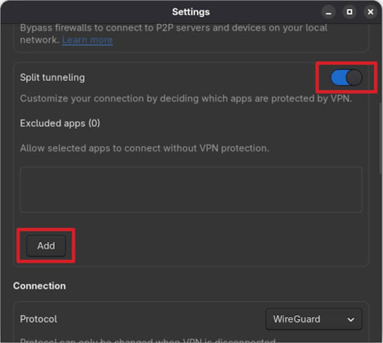
Proton VPN Enhances Linux App with Beta Split Tunneling Functionality Linux users of Proton VPN can now access the split tunneling feature in beta, marking a significant upgrade to the platform's capabilities on this operating system. The new functionality allows subscribers to choose which applications or IP addresses route through the VPN connection, while allowing other traffic to bypass...
Crystal Palace now face a serious test on the road to the Conference League Final 2026. Their opponent has won again, and that matters because form can change the mood before kickoff. A fresh win gives belief, rhythm, and a stronger voice in the dressing room. Palace, though, can still use the situation well. Many football fans are getting ready to watch the Conference League Final. People...

South Goa’s quiet beaches and scenic landscapes make it a perfect destination for a relaxing holiday. Choosing Boutique Resorts in South Goa allows travelers to experience comfort and style in a peaceful setting. These resorts focus on creating a personalized experience that feels both luxurious and homely. A stay at Boutique Resorts in South Goa offers more than just...