Specialty Polymers for Semiconductors: The Invisible Infrastructure Holding Together Every Advanced Fab, Wafer, Chip Package, and AI Compute Buildout
A semiconductor fab looks like a steel-and-silicon cathedral, but its reliability often depends on materials measured in microns, parts per billion, and nanometers. Specialty Polymers for Semiconductors sit inside this hidden layer. They are not visible like EUV scanners, deposition chambers, etchers, or wafer probers, but they decide whether a fab can run 24 hours a day with chemical purity, plasma resistance, low outgassing, dimensional stability, and particle control.
Semple Request At: https://datavagyanik.com/reports/global-specialty-polymers-for-semiconductors-market/
The infrastructure story starts with scale. A modern 300mm fab can process 30,000 to 100,000 wafer starts per month. Each wafer may pass through 700 to 1,200 process steps in advanced logic and memory flows. If even 0.01% of polymer-contact points release particles, ions, extractables, or micro-contamination, the yield loss can move from engineering noise to financial damage. At a $15,000 to $25,000 processed wafer value for advanced nodes, a 1% yield impact across 50,000 wafers per month can translate into $7.5 million to $12.5 million of monthly value at risk.
That is why Specialty Polymers for Semiconductors are infrastructure materials, not commodity plastics. They appear in chemical delivery tubing, wafer carriers, gaskets, seals, CMP retaining rings, electrostatic chuck components, photoresist systems, advanced packaging dielectrics, filtration housings, wet process tanks, connector parts, cleanroom handling systems, and high-temperature process components. In a single fab, polymer-based components may touch ultrapure water, hydrofluoric acid, sulfuric acid, hydrogen peroxide, ammonium hydroxide, solvents, photoresist chemistries, slurry systems, plasma environments, and packaging resins.
The first application map is chemical infrastructure. Semiconductor manufacturing consumes millions of liters of ultrapure water per day in large fabs, and wet process lines operate with aggressive acids and bases. Fluoropolymers such as PFA, PTFE, FEP, ETFE, and PVDF dominate this layer because they can resist corrosive fluids while limiting extractables. A 300mm wet bench installation can contain hundreds of meters of tubing, dozens of valves, multiple tanks, and hundreds of seals. Across a multi-module fab, polymer material value in chemical delivery and wet processing can easily exceed several million dollars before the first wafer moves through production.
Specialty Polymers for Semiconductors also serve as the contamination firewall. In older industrial plastics, sodium, potassium, calcium, chloride, metallic residues, and organic leachables may be tolerable. In semiconductor fabs, contamination is counted in parts per billion or lower. A polymer seal that performs well mechanically but sheds trace ions can damage gate oxide integrity, reduce device reliability, or create latent defects. For nodes below 7nm, and for high-bandwidth memory stacks used in AI accelerators, defect tolerance keeps shrinking because one bad layer can compromise a device containing billions of transistors.
The second application map is thermal and mechanical stability. Polyimide, PEEK, PPS, LCP, PAI, PEI, and high-purity fluoropolymers are selected where temperature, dimensional control, and low outgassing matter. A polymer component inside wafer handling equipment may experience repeated thermal cycles, mechanical friction, robotic motion, and cleanroom sterilization. A carrier, clamp, guide, or insulating part cannot warp by even a small fraction of a millimeter if it affects wafer positioning. At 300mm wafer scale, a 100-micron mechanical deviation can become a yield issue when alignment budgets are already tight.
Specialty Polymers for Semiconductors become even more important when manufacturing moves from planar scaling to 3D architectures. In NAND, layer counts have moved beyond 200 layers. In advanced logic, gate-all-around structures require tighter process control. In DRAM and HBM, stacking and packaging density are increasing. Every transition adds more process steps, more chemical exposure, more plasma exposure, and more packaging interfaces. If a chip architecture becomes more three-dimensional, the polymer exposure map also becomes more three-dimensional.
DataVagyanik estimates the global Specialty Polymers for Semiconductors market at USD 5.42 billion in 2026, with the market forecast to reach USD 9.86 billion by 2032, expanding at a 10.5% CAGR. This estimate includes semiconductor-grade fluoropolymers, polyimides, PEEK, PPS, LCP, photoresist-linked polymer systems, advanced packaging polymers, CMP-related polymer components, seals, tubing, wafer handling materials, filtration-compatible polymer housings, and process equipment polymer parts. The strongest revenue pull is expected from advanced logic, HBM, 3D NAND, AI accelerator packaging, and new fabs moving from qualification to volume production between 2026 and 2032.
The third application map is lithography and patterning. Photoresist chemistry depends on polymer backbones, dissolution behavior, acid diffusion control, adhesion, film uniformity, and etch resistance. For EUV lithography, the issue is not only resolution; it is stochastic defect control. A small variation in polymer chemistry can affect line-edge roughness, bridge defects, and missing contacts. If an advanced fab runs tens of thousands of wafers per month, even a few additional defects per square centimeter can reshape the cost curve of a node.
This is where Specialty Polymers for Semiconductors become part of transistor economics. The industry often talks about EUV scanners costing more than $150 million each, but scanner productivity depends on chemical stacks that behave predictably at nanometer dimensions. A photoresist film may be only tens of nanometers thick, yet it determines whether a multi-billion-dollar fab can print patterns consistently. The polymer is physically thin, but financially heavy.
The fourth use case sits in CMP, where wafers are polished with slurry, pressure, pads, rings, and tight endpoint control. CMP retaining rings made from engineered polymers must resist abrasion, maintain dimensional stability, and avoid particle generation. A single CMP tool may process hundreds of wafers daily. Across copper, tungsten, oxide, and dielectric polishing steps, polymer performance affects wafer planarity. If planarity fails, downstream lithography and deposition steps lose control. In this use case, Specialty Polymers for Semiconductors are not passive parts; they are process-control materials.
The fifth use case is advanced packaging. AI chips, GPUs, HBM modules, chiplets, silicon interposers, redistribution layers, fan-out packages, and 2.5D/3D integration all increase demand for dielectric films, encapsulation materials, temporary bonding materials, underfills, mold compounds, and stress-buffer polymers. A high-end AI package can contain multiple chips, thousands of micro-bumps, dense redistribution layers, and thermal interfaces packed into a few square centimeters. The more heterogeneous the package becomes, the more polymer interfaces it contains.
Specialty Polymers for Semiconductors are therefore shifting from fab support materials to performance-enabling materials. In a conventional package, polymer value may be modest. In advanced packaging, polymer value rises because electrical insulation, warpage control, thermal reliability, adhesion, stress management, and moisture resistance all become critical. A chiplet package that fails reliability testing after thermal cycling does not fail because silicon is weak; it often fails because interfaces, stresses, and material expansion coefficients are not balanced.
The infrastructure investment timeline supports this material pull. Global 300mm fab equipment spending is moving above the $130 billion level in 2026, and industry-body forecasts indicate continued expansion into 2027 as AI, memory, logic, and regional semiconductor self-sufficiency programs keep capex elevated. Every new fab does not only buy tools; it buys kilometers of chemical lines, thousands of cleanroom polymer components, filtration systems, FOUPs, valves, O-rings, wafer-contact parts, CMP consumables, and packaging material systems. A $10 billion fab may allocate only a small percentage to specialty polymer-linked materials and components, but even 0.5% to 1.0% converts into $50 million to $100 million of polymer-related infrastructure demand over buildout and ramp-up.
This is the core adoption logic for Specialty Polymers for Semiconductors: demand grows with wafer starts, but value grows faster with process complexity. A mature-node fab may need chemical resistance and clean handling. An advanced-node fab needs chemical resistance, plasma durability, ultra-low contamination, thermal control, lithographic precision, and packaging reliability at the same time. The polymer bill does not rise linearly with wafers; it rises with the number of critical interfaces per wafer.
From a manufacturer perspective, the market is concentrated around material science companies with semiconductor qualification discipline. DuPont, Entegris, Solvay, Arkema, Chemours, Daikin, AGC, Toray, Sumitomo Bakelite, Resonac, Mitsui Chemicals, Shin-Etsu Chemical, JSR, Tokyo Ohka Kogyo, and Zeon are relevant because they do not merely sell polymers; they sell controlled purity, repeatability, lot traceability, clean manufacturing, and application qualification. In semiconductors, a polymer supplier is not accepted because its datasheet looks strong. It is accepted after qualification cycles that can run 6 to 24 months depending on application criticality.
The technical barrier is qualification cost. A polymer part used outside the wafer path can qualify faster. A polymer touching process chemicals, wafers, photoresist stacks, or advanced package interfaces faces deeper scrutiny. Material change notices, extractable testing, plasma exposure studies, ionic contamination checks, mechanical endurance, thermal aging, and customer-specific validation are part of adoption. This slows supplier switching but protects incumbents. Once Specialty Polymers for Semiconductors are qualified into a critical process, replacement is not a purchasing decision; it becomes a process engineering decision.
That is why the market behaves differently from general engineering plastics. Price matters, but failure cost matters more. A polymer gasket costing a few dollars can sit inside a tool module worth several million dollars. A polymer film costing cents per unit can protect a package worth hundreds or thousands of dollars. A CMP ring or wafer-handling component may look like a consumable, but if it reduces scratches or particles, it pays for itself through yield preservation.
In semiconductor economics, the cheapest polymer is rarely the lowest-cost polymer. The lowest-cost material is the one that protects uptime, yield, and qualification stability. This is the practical reason Specialty Polymers for Semiconductors are becoming one of the quietest but most strategic material categories in the AI-era chip supply chain.
Specialty Polymers for Semiconductors: From Cleanroom Hardware to AI Packaging, the Material Layer Where Yield Is Protected
The regional infrastructure story is equally quantified. Taiwan, South Korea, the United States, Japan, China, Singapore, Germany, and India are not building the same semiconductor ecosystem. Taiwan and South Korea are concentrated around advanced foundry, memory, and packaging intensity. The United States is adding logic, memory, and equipment-linked capacity. Japan remains strong in materials, chemicals, wafers, photoresists, fluoropolymers, and packaging supply chains. China is expanding mature-node, memory, power semiconductor, display driver, and domestic materials qualification. India is entering through assembly, testing, packaging, compound semiconductors, and early-stage fab-linked infrastructure. Each geography creates a different pull for Specialty Polymers for Semiconductors.
A front-end logic fab demands the highest purity and process compatibility. A memory fab demands high-volume repetition and tool uptime. A power semiconductor fab demands thermal resistance, chemical resistance, and cost-effective process integration. An outsourced semiconductor assembly and test facility demands underfills, mold compounds, die attach films, redistribution polymers, trays, carriers, and test-socket materials. This means Specialty Polymers for Semiconductors do not follow one demand curve. They follow at least four demand curves: wafer fabrication, process equipment, lithography chemistry, and advanced packaging.
The capital intensity of this demand is visible in fab math. A 40,000-wafer-per-month 300mm fab can require 1,000 to 1,500 major process and support tools when deposition, etch, lithography, clean, CMP, metrology, inspection, implantation, diffusion, and automation modules are counted. If only 60% of these tool categories contain critical polymer components, that still places polymer-qualified parts inside 600 to 900 tool environments. When each environment has tubing, seals, valve parts, chamber components, wafer contact materials, or consumable polymer interfaces, the infrastructure footprint becomes large before production volume is considered.
Specialty Polymers for Semiconductors also ride on the cleanroom buildout. A large fab can occupy 100,000 to 250,000 square meters of built-up space, with cleanroom space representing a smaller but much more expensive portion. Cleanrooms require HEPA and ULPA filtration, antistatic surfaces, high-purity ducts, chemical-resistant flooring systems, polymer-based seals, filters, containment materials, and clean-compatible handling products. The polymer value per square meter is not high in general construction terms, but in semiconductor-grade controlled environments, the required certification, low shedding, and chemical compatibility multiply the value.
The next story is about wafer movement. A 300mm wafer is physically fragile, financially dense, and contamination-sensitive. FOUPs, wafer carriers, trays, robotic end-effectors, guides, cushions, and handling systems rely on high-performance polymers. A fab running 50,000 wafer starts per month may move wafers millions of times across process steps during a year. Even a microscopic scratch rate of 0.001% becomes meaningful when multiplied by millions of handling events. This is where Specialty Polymers for Semiconductors function as mobility infrastructure for wafers.
At the equipment level, polymer selection is application-specific. Fluoropolymers dominate aggressive chemical transfer because they resist acids, bases, oxidizers, and solvents. Polyimides dominate high-temperature insulation, films, and advanced packaging dielectrics. PEEK and PAI serve mechanical wear, strength, and dimensional stability applications. PPS is used where chemical resistance and cost balance matter. LCP supports precision electrical and connector applications where low moisture uptake and dimensional stability are required. Epoxy, silicone, benzocyclobutene, polybenzoxazole, and other dielectric polymer systems support packaging, passivation, stress buffer, and redistribution layers.
This is why Specialty Polymers for Semiconductors should not be treated as one material family. The market is a toolkit. A wet etch module, EUV photoresist stack, CMP tool, wafer carrier, chiplet package, and thermal management assembly may all use polymers, but the performance criteria are different. Chemical inertness, dielectric constant, glass transition temperature, coefficient of thermal expansion, moisture absorption, plasma erosion rate, ion purity, elastic modulus, and particle generation all become selection filters.
The use case mapping becomes sharper when viewed by semiconductor node and package type. Mature-node analog, power, and microcontroller fabs use specialty polymers mainly for chemical handling, equipment parts, seals, carriers, and standard packaging materials. Advanced logic uses higher-value polymers for lithography, plasma exposure, contamination control, and wafer handling. Memory uses large-volume polymer demand across high-throughput process tools and packaging. AI accelerators use advanced packaging polymers with higher reliability requirements because large die sizes and multi-die architectures intensify warpage and thermal stress.
Specialty Polymers for Semiconductors therefore gain the highest value density in two places: the cleanest part of front-end wafer fabrication and the most complex part of back-end advanced packaging. In front-end, the polymer must not contaminate. In back-end, the polymer must hold complex structures together under electrical, thermal, and mechanical stress. One side protects the transistor. The other side protects the package.
Advanced packaging deserves its own infrastructure lens. A conventional wire-bonded package may contain a simpler polymer stack: mold compound, die attach material, substrate resin, and basic encapsulation. A chiplet package may contain underfill, temporary bonding adhesive, release layers, redistribution dielectric, passivation polymers, substrate build-up films, thermal interface materials, and encapsulants. A single high-end package can have 5 to 10 polymer-relevant material layers compared with 2 to 4 in a conventional package. That step-up is the reason packaging is becoming one of the strongest growth engines for Specialty Polymers for Semiconductors.
The AI compute story strengthens this. Training clusters require GPUs, AI accelerators, HBM, networking chips, power management chips, optical modules, and advanced substrates. One AI server can contain multiple high-value semiconductor packages. Each package depends on polymer materials for insulation, stress relief, adhesion, encapsulation, and thermal pathways. When hyperscale data-center capex moves into hundreds of billions of dollars globally, the polymer exposure is not direct but embedded: more accelerators mean more HBM stacks, more advanced packages, more substrates, more underfills, and more thermal materials.
From 2026 onward, the strongest pull will come from HBM and 2.5D integration. HBM stacks require precise bonding, dielectric materials, encapsulation, and stress control. As HBM moves from 8-high to 12-high and beyond, vertical stack reliability becomes more difficult. More layers mean more interfaces. More interfaces mean more chances for delamination, cracking, warpage, moisture ingress, or thermal fatigue. Specialty Polymers for Semiconductors become the interface insurance policy for this architecture.
The technical quantification is straightforward. Silicon has a very low coefficient of thermal expansion, while organic substrates and polymer materials expand more under heat. When a package cycles between operating and idle temperatures thousands of times, mismatch creates stress. A polymer material must absorb some stress without losing adhesion or electrical performance. If a package operates near 80°C to 110°C in high-performance environments and experiences repeated thermal cycling, the wrong polymer can create failure modes long before the chip’s electrical design becomes obsolete.
The supplier ecosystem is also shaped by purity infrastructure. Semiconductor-grade polymer production requires clean compounding, controlled feedstock, metal contamination testing, filtration, clean packaging, and traceable batches. A normal industrial polymer plant is not enough. Suppliers need dedicated or specially controlled lines, quality systems, application labs, and customer-specific data packages. This is why the effective supplier base is smaller than the apparent polymer industry. Many companies can manufacture high-performance polymers; fewer can consistently supply Specialty Polymers for Semiconductors.
A useful way to quantify supplier relevance is by qualification depth. Tier 1 relevance belongs to companies supplying direct wafer-process materials, photoresist systems, fluoropolymer components, or advanced packaging polymers. Tier 2 relevance belongs to compounders and component manufacturers making qualified parts from high-performance resins. Tier 3 relevance belongs to distributors, converters, and fabricators serving less critical cleanroom and tool-support applications. The closer the polymer sits to wafer, chemistry, plasma, or package interfaces, the higher the qualification barrier and margin potential.
There is also a replacement cycle story. Polymer tubes, seals, CMP rings, filters, carriers, and handling components are not one-time capital items. Some are replaced on maintenance schedules measured in weeks or months. Others last years but must be replaced during tool service or fab expansion. This creates a hybrid revenue model: initial fab buildout creates infrastructure demand, while wafer production creates recurring consumable demand. Specialty Polymers for Semiconductors therefore benefit from both capex cycles and fab utilization cycles.
In a downturn, new fab spending can slow, but operating fabs still consume process materials and replacement components. In an upcycle, both new buildout and utilization rise together. That gives the category more resilience than pure equipment exposure. A lithography scanner sale can be cyclical. A polymer seal, CMP component, wafer carrier, underfill, dielectric film, or chemical tubing line has a more distributed demand pattern across construction, ramp-up, and production.
Localization is now becoming part of the story. The United States wants secure materials for domestic fabs. Japan wants to retain leadership in chemicals and polymers. South Korea wants local support for memory and packaging. China wants domestic substitution. India wants to build semiconductor assembly and eventually upstream material capability. Europe wants semiconductor resilience around automotive, power electronics, and industrial chips. This geopolitical shift gives Specialty Polymers for Semiconductors a new strategic label: supply-chain security material.
However, localization is not simple. Semiconductor customers do not localize a polymer just because it is available domestically. They localize after it passes purity, reliability, tool compatibility, and process repeatability tests. For a critical application, switching from an incumbent imported polymer to a new local material can take 12 to 36 months. That means the opportunity is large, but the adoption clock is slow.
India illustrates the gap. The country can build demand through OSAT, ATMP, power electronics, compound semiconductor, and electronics manufacturing. But semiconductor-grade fluoropolymers, advanced photoresist polymers, high-end packaging dielectrics, and ultra-high-purity process polymers require deeper upstream chemistry, purification, testing, and clean manufacturing capability. India’s near-term opportunity is stronger in packaging polymers, cleanroom-compatible components, trays, carriers, cable insulation, selected seals, and downstream fabrication than in the most demanding front-end polymer chemistries.
For manufacturers, the commercial strategy should be application-led, not resin-led. Selling PEEK, PFA, polyimide, PPS, or LCP by chemistry misses the semiconductor buyer’s decision logic. The buyer asks: does it reduce particles, extend maintenance intervals, survive plasma, pass extractables testing, maintain dielectric performance, reduce warpage, or protect yield? Specialty Polymers for Semiconductors win when they are positioned as risk-reduction materials.
The final theme is that semiconductor scaling is no longer only about smaller transistors. It is about more layers, more interfaces, more packages, more thermal density, more chemical steps, and more yield sensitivity. That makes the material stack as strategic as the equipment stack. Fabs will keep buying bigger tools, but those tools will keep depending on smaller, cleaner, more stable polymer components.
In this sense, Specialty Polymers for Semiconductors are the quiet operating system of semiconductor infrastructure. They route chemicals, protect wafers, stabilize tools, enable patterning, absorb stress, insulate packages, and preserve yield. Their value is not measured only by kilograms sold. It is measured by avoided defects, protected uptime, qualified processes, and the ability to manufacture chips at volumes where one particle, one ion, or one warped package can decide millions of dollars of output.
Semple Request At: https://datavagyanik.com/reports/global-specialty-polymers-for-semiconductors-market/
Категории
Больше
Retinal swelling is a serious ocular condition that can affect visual clarity and overall retinal function if not diagnosed at an early stage. Swelling occurs when fluid accumulates within retinal tissues, causing structural changes that may interfere with the retina’s ability to process visual information effectively. In many cases, the condition develops gradually and may not produce...
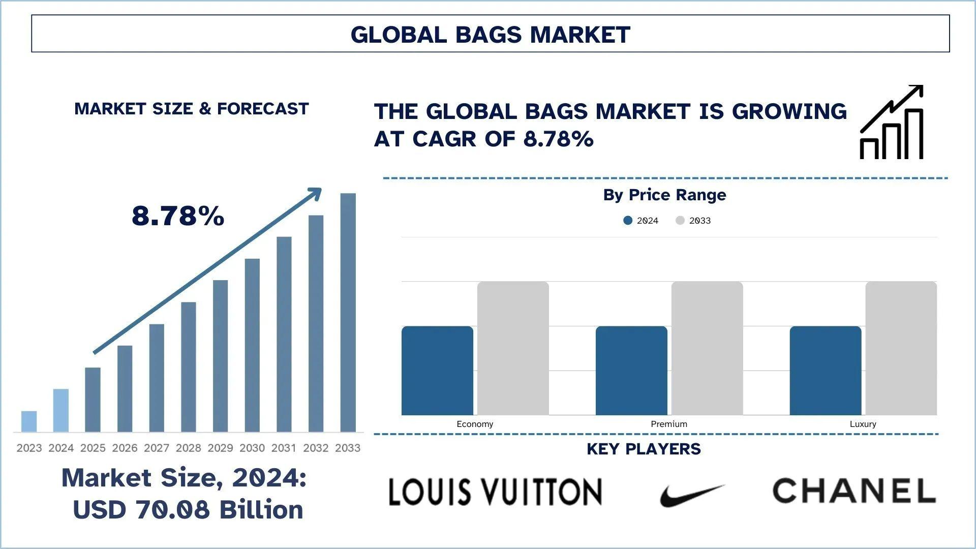
According to UnivDatos analysis, rising fashion consciousness, increasing travel and tourism activities, growing demand for functional and lifestyle accessories, expanding e-commerce penetration, rising disposable income, and increasing preference for sustainable and customized products are the major factors driving the growth of the global bags market. As per their “Bags Market”...
Woont u in Zoersel en heeft u dringend een slotenmaker nodig? Een professionele slotenmaker in Zoersel staat klaar om u snel en efficiënt te helpen bij buitensluiting, kapotte sloten of inbraakschade. In een groene en residentiële gemeente zoals Zoersel is veiligheid een belangrijke prioriteit voor gezinnen, zelfstandigen en bedrijven. 24/7 Hulp bij Buitensluiting Een buitensluiting...
Did you know that over 60% of renters prioritize flexibility in lease terms? In Greensboro, this trend is shaping the way apartments are designed, catering to your need for adaptability and convenience. With options for both short- and long-term leases, alongside robust security measures and dedicated professional services, these apartments aim to simplify your living experience. But how do...
A few years ago, most shopping apps worked in a simple way. You searched for a product, added it to the cart, and placed an order. Today, things feel very different. Apps now suggest products, understand your choices, and even predict what you may want next. This shift is mainly because of AI, which is now a key part of ecommerce app development. As competition grows,...