


Why Flat No-leads Package Is Quietly Becoming the Infrastructure Backbone of High-Density Electronics in the AI and Electrification Era

Why Flat No-leads Package Is Quietly Becoming the Infrastructure Backbone of High-Density Electronics in the AI and Electrification Era
The modern electronics industry is no longer competing only on computing power. It is competing on space efficiency, thermal management, manufacturing speed, and long-term reliability. Every new smartphone, electric vehicle controller, industrial automation board, wearable sensor, networking switch, and medical monitoring device demands more functions within smaller footprints. This engineering shift has elevated the Flat No-leads Package from a standard semiconductor package into one of the most important infrastructure technologies supporting global electronics manufacturing.
A decade ago, semiconductor innovation focused primarily on transistor scaling. Today, package architecture contributes a significant share of total device performance because electrical losses, heat dissipation, signal integrity, and assembly efficiency increasingly determine system capability. The Flat No-leads Package addresses these requirements by eliminating protruding leads while creating short electrical paths that reduce parasitic inductance and improve thermal conductivity. Manufacturers now evaluate package selection almost as carefully as silicon selection itself.
More than 70% of newly designed compact electronic modules emphasize board-space optimization as a primary engineering objective. Since packaging typically occupies between 25% and 45% of the overall component footprint, the adoption of the Flat No-leads Package directly influences PCB density, manufacturing yield, and system reliability. As PCB layer counts continue increasing from conventional 4-layer designs toward 10 to 20-layer high-density architectures, package efficiency has become an enabling technology rather than a supporting feature.
Electronics infrastructure investment reflects this transformation. Global semiconductor packaging facilities continue expanding advanced assembly capacity with billions of dollars allocated toward automation, inspection systems, copper clip bonding, laser marking, wafer-level handling, and high-speed surface-mount production lines. A modern packaging facility may process well above 100 million semiconductor packages annually while maintaining defect levels measured in only a few parts per million. Within these production environments, the Flat No-leads Package has become one of the highest-volume package formats because it combines manufacturing simplicity with exceptional electrical performance.
Infrastructure development is equally visible inside PCB assembly plants. Modern SMT production lines routinely place more than 80,000 components every hour using automated optical inspection, X-ray verification, solder paste inspection, and AI-assisted defect analytics. Since the Flat No-leads Package features exposed thermal pads and compact geometries, manufacturers increasingly optimize stencil design, solder volume, and reflow temperature profiles specifically around this package family. The result is improved production consistency and lower assembly costs across consumer electronics, automotive electronics, industrial control systems, and communication equipment.
The transition toward electrified transportation has further accelerated deployment. A single battery electric vehicle may integrate between 2,000 and 3,500 semiconductor devices controlling battery management, lighting, infotainment, power steering, motor control, charging systems, radar, cameras, and advanced driver assistance systems. Many analog ICs, power management chips, sensor interfaces, communication controllers, and RF components inside these modules are increasingly delivered through the Flat No-leads Package because of its superior heat transfer characteristics and compact footprint.
Industrial automation presents another compelling infrastructure story. Modern smart factories continue increasing sensor density to improve predictive maintenance, machine vision, robotics, and energy management. A medium-sized automated manufacturing plant can deploy over 20,000 connected sensing points monitoring vibration, pressure, current, temperature, and positioning. These sensing nodes require compact integrated circuits capable of operating continuously under demanding thermal conditions. The Flat No-leads Package supports these requirements by minimizing electrical resistance while maintaining mechanical robustness under extended operational cycles.
The communications sector demonstrates a similar evolution. Fifth-generation wireless infrastructure, Wi-Fi 7 equipment, edge computing hardware, industrial gateways, and enterprise networking switches demand increasingly compact RF front-end modules and high-frequency analog components. Because signal integrity becomes increasingly sensitive at higher frequencies, reducing package parasitics becomes essential. Engineers therefore frequently select the Flat No-leads Package when designing compact RF amplifiers, filters, clock generators, voltage regulators, and interface controllers that operate across demanding frequency ranges.
Healthcare electronics provide another rapidly expanding application landscape. Portable ultrasound systems, wearable health monitors, insulin pumps, diagnostic analyzers, and patient monitoring devices continue shrinking while increasing processing capability. Device designers typically pursue reductions of 20% to 40% in PCB area across each new product generation without compromising reliability. This engineering objective naturally supports broader adoption of the Flat No-leads Package, particularly in analog front-end circuits, sensor interfaces, battery management systems, and wireless communication modules.
One of the defining strengths of the Flat No-leads Package lies in thermal engineering. Traditional leaded packages transfer heat through leads and package surfaces, while exposed-pad no-lead structures establish a direct thermal path into the PCB. Depending on board design and copper thickness, thermal resistance may improve substantially compared with older packaging alternatives. Lower junction temperatures translate into extended semiconductor lifespan, improved reliability, and greater power efficiency, making thermal performance a measurable economic advantage rather than merely a technical specification.
This engineering advantage becomes increasingly important as AI processing expands toward edge devices. Instead of sending every computation to cloud infrastructure, manufacturers increasingly process data locally within cameras, industrial controllers, medical instruments, autonomous robots, and smart appliances. Edge AI processors generate higher thermal loads inside physically smaller products. Efficient package architecture therefore becomes a prerequisite for sustained performance. The Flat No-leads Package enables engineers to manage these thermal constraints without significantly increasing product dimensions.
The economics of manufacturing reinforce this transition. Compact packages reduce material consumption, improve reel density during shipping, and support automated pick-and-place operations at extremely high throughput. Lower package height also enables thinner consumer products, while simplified geometry contributes to manufacturing repeatability. Across high-volume production exceeding tens of millions of units annually, even fractional reductions in assembly cycle time can translate into millions of dollars in operational savings. Consequently, procurement teams increasingly evaluate the Flat No-leads Package not only for technical performance but also for production efficiency.
According to Staticker, the Flat No-leads Package market size in 2026 is positioned for a strong expansion trajectory through the forecast period, supported by accelerating semiconductor packaging investments, increasing AI hardware production, automotive electronics growth, industrial automation, and compact consumer device manufacturing. Staticker attributes future market expansion to sustained demand for thermally efficient package architectures, higher semiconductor content per electronic system, and continuous infrastructure investments in advanced packaging technologies across Asia-Pacific, North America, and Europe.
Another factor driving the Flat No-leads Package ecosystem is the rapid expansion of outsourced semiconductor assembly and test infrastructure. OSAT providers continue investing in automated die attach systems, precision molding equipment, laser singulation, advanced inspection platforms, and AI-powered quality analytics. Production facilities increasingly operate with digital manufacturing systems capable of real-time yield monitoring, predictive maintenance, and automated defect classification. These investments allow manufacturers to maintain consistently high production volumes while meeting the stringent quality standards required for automotive, industrial, aerospace, and medical electronics.
Request for customization: https://staticker.com/reports/flat-no-leads-package-market/
Κατηγορίες
Διαβάζω περισσότερα
Elegant Collections is your destination for premium home furnishings if you're searching for a dependable Furniture Store Geelong. We offer a wide selection of stylish sofas, dining furniture, bedroom collections, office furniture, and decorative pieces to enhance every corner of your home. As a leading Furniture Store Geelong, we combine quality materials with elegant designs to provide...

According to the latest report published by Data Bridge Market Research, the Gloves Market The global Gloves market size was valued at USD 26.96 billion in 2024 and is expected to reach USD 55.33 billion by 2032, at a CAGR of 9.40% during the forecast period In this persuasive Gloves Market report, market analysis and market segmentation is...
The global coal bed methane (CBM) market is poised for significant expansion over the next decade, driven by increasing demand for cleaner-burning fuels and the growing focus on unconventional gas resources. The market is projected to grow from approximately USD 18.5 billion in 2026 to around USD 33.8 billion by 2036, registering a CAGR of nearly 6.2%, according to the...
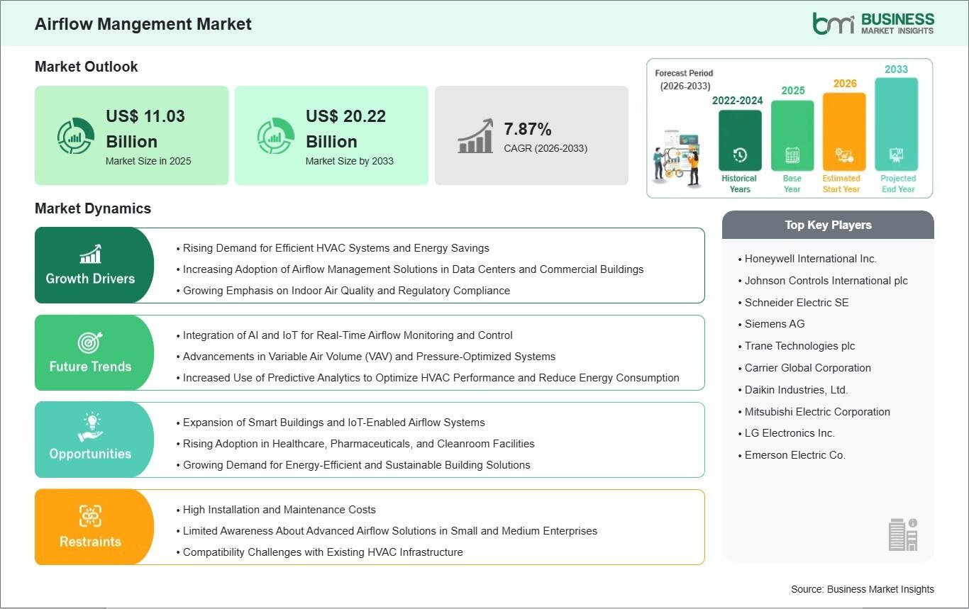
The Airflow Management Industry is undergoing a rapid structural expansion globally, driven by the explosive growth of hyperscale data centers, the escalating demand for energy-efficient commercial infrastructure, and the continuous push toward sustainable, net-zero operations. As industries scale up high-density computing capabilities for AI and cloud services, regulating thermal dynamics has...
Healthcare is about more than simply filling prescriptions—it’s about building relationships, promoting wellness, and making quality care easily accessible. Across the United States, more people are turning to community pharmacies that offer personalized services, professional guidance, and convenient healthcare solutions under one roof. Texan Pharmacy is proud to provide...
