Logic Test Probe Card Infrastructure: The Silent Network That Decides the Yield of Every Advanced Semiconductor
Logic Test Probe Card Infrastructure: The Silent Network That Decides the Yield of Every Advanced Semiconductor
Every semiconductor breakthrough begins long before a chip reaches a smartphone, AI server, automotive controller, or industrial robot. Hidden between wafer fabrication and final packaging exists a testing infrastructure that determines whether billions of transistors can actually perform as designed. At the center of this infrastructure sits the Logic Test Probe Card market, an engineering platform that rarely appears in headlines yet directly influences yield, reliability, and manufacturing economics.
Modern semiconductor fabs routinely process wafers containing hundreds or even thousands of individual dies. A single advanced logic wafer may represent weeks of processing, more than 1,000 manufacturing steps, and investment exposure measured in thousands of dollars before testing even begins. The Logic Test Probe Card becomes the first physical interface that validates whether these devices are functional.
The importance of the Logic Test Probe Card has expanded dramatically over the last decade. While transistor dimensions have shrunk by more than 90% compared with legacy nodes, test complexity has moved in the opposite direction. Advanced logic devices now integrate CPU cores, AI accelerators, memory controllers, security modules, and communication interfaces within a single die. Testing such complexity requires a highly engineered Logic Test Probe Card capable of handling thousands of simultaneous electrical connections with micron-level precision.
Building the Infrastructure Behind Semiconductor Validation
A semiconductor fab producing 50,000 wafer starts per month may test several million individual devices before packaging. This volume creates an extensive infrastructure ecosystem around the Logic Test Probe Card.
The infrastructure begins with probe-card design centers where electrical engineers model signal integrity, impedance behavior, and contact resistance. Modern designs often support thousands of contact points, compared with only a few hundred in earlier generations.
Manufacturing infrastructure follows. Probe card production requires precision machining, MEMS fabrication capabilities, advanced ceramics, multilayer substrates, and automated optical inspection systems. Alignment tolerances are frequently measured in microns rather than millimeters. A positional deviation smaller than a human hair can impact testing accuracy.
The third layer is operational infrastructure. Semiconductor manufacturers deploy fleets of automated test equipment operating continuously across multiple shifts. Each tester relies on a dedicated Logic Test Probe Card configuration optimized for specific logic devices. In high-volume environments, utilization rates often exceed 85%, making probe-card reliability a measurable contributor to fab productivity.
Industry spending trends have reflected this reality. As advanced-node production expanded for AI processors, automotive semiconductors, and high-performance computing devices, manufacturers increased investments in test-cell modernization, contact technology improvements, and probe-card maintenance systems. The result is an ecosystem where testing infrastructure increasingly represents a strategic competitive advantage rather than a downstream quality-control function.
Why Logic Devices Create Unique Testing Challenges
Unlike analog or power semiconductors, logic chips generate extraordinarily large testing datasets.
A contemporary processor may contain tens of billions of transistors. While not every transistor is tested individually, manufacturers execute extensive functional, parametric, and structural tests. The Logic Test Probe Card serves as the gateway through which these measurements are collected.
Consider signal pathways. Modern logic devices operate at frequencies measured in gigahertz. Small variations in contact quality can distort measurements, increase error rates, or create false failures. Consequently, the Logic Test Probe Card must maintain electrical consistency across thousands of touchdown cycles.
Testing density has also increased significantly. In many advanced applications, manufacturers seek to maximize parallel testing efficiency by evaluating multiple dies simultaneously. This means a single Logic Test Probe Card may support dramatically higher channel counts than previous generations, reducing cost per tested die while increasing throughput.
Quantitatively, if parallelism doubles, testing cost per device can decline substantially without increasing tester footprint. Across millions of units annually, these efficiencies influence profitability, manufacturing capacity, and supply-chain responsiveness.
Logic Test Probe Card Market Size and the Growth Trajectory Toward Advanced Computing
According to Staticker, the Logic Test Probe Card market in 2026 is expected to demonstrate continued expansion driven by advanced-node semiconductor production, artificial intelligence processors, automotive electronics, and high-performance computing applications. The market's growth forecast remains closely linked to rising wafer complexity, increasing test intensity, and broader adoption of multi-die architectures. Staticker indicates that infrastructure investments across wafer testing ecosystems are expected to outpace several other semiconductor support segments through the forecast period, with demand increasingly concentrated around high-pin-count and advanced logic testing environments rather than legacy semiconductor applications.
Application Mapping: Where the Logic Test Probe Card Creates Measurable Value
The value of a Logic Test Probe Card becomes clear when mapped across semiconductor end-use sectors.
In AI accelerators, testing accuracy directly affects deployment reliability. A single defective compute die entering a data-center environment can create operational inefficiencies far exceeding its manufacturing cost. Therefore, comprehensive wafer-level validation becomes essential.
In automotive electronics, reliability requirements are even stricter. Advanced driver-assistance systems may process millions of calculations every second. The Logic Test Probe Card helps manufacturers identify latent defects before chips enter safety-critical environments.
Consumer electronics provide another scale-driven example. Smartphone processor volumes can reach tens of millions of units annually. Even a 1% improvement in yield may translate into hundreds of thousands of additional sellable devices. Here, the Logic Test Probe Card contributes directly to manufacturing economics.
Industrial automation applications add another dimension. Logic controllers operating in factories often remain deployed for years. Testing infrastructure must therefore prioritize consistency and long-term performance verification. The Logic Test Probe Card enables these validation workflows through repeatable electrical contact performance.
Quantifying the Engineering Behind Contact Technology
One of the most overlooked aspects of the Logic Test Probe Card is contact engineering.
A probe card must repeatedly establish electrical connections with wafer pads while minimizing wear and maintaining measurement accuracy. In production environments, contact structures may experience hundreds of thousands or even millions of touchdowns throughout operational life.
Engineers optimize multiple variables simultaneously:
-
Contact resistance stability
-
Mechanical durability
-
Thermal performance
-
Signal integrity
-
Alignment accuracy
-
Cleaning efficiency
For advanced logic devices, even small improvements in contact consistency can generate significant manufacturing benefits. If testing errors are reduced by fractions of a percentage point across millions of devices, the resulting yield gains become economically meaningful.
The transition toward heterogeneous integration further amplifies these requirements. Multi-chip architectures create additional interfaces and validation scenarios, increasing the role of the Logic Test Probe Card in manufacturing workflows.
The Emerging Theme: Testing as a Strategic Manufacturing Asset
Historically, semiconductor testing was often viewed as a downstream verification step. That perception is changing.
Today, manufacturers increasingly treat testing infrastructure as a strategic asset influencing capacity utilization, yield performance, product quality, and time-to-market. Within this framework, the Logic Test Probe Card functions as a critical bridge between fabrication and commercialization.
As transistor counts rise, packaging architectures become more sophisticated, and AI-driven semiconductor demand accelerates, the complexity handled by every Logic Test Probe Card will continue increasing. The future of semiconductor manufacturing may ultimately depend not only on how efficiently chips are fabricated, but also on how intelligently they are validated before reaching the market.
Request for customization: https://staticker.com/reports/logic-test-probe-card-market/
Categorias
Leia mais
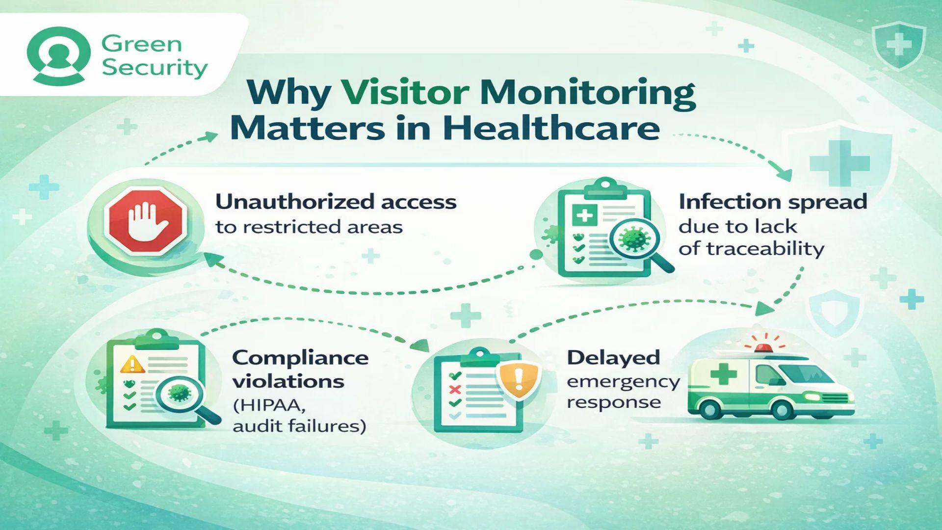
Introduction Visitor monitoring in healthcare is no longer just a front-desk function—it’s a critical safety infrastructure. Hospitals today manage thousands of visitors, vendors, and contractors daily, making real-time visibility essential. Visitor monitoring refers to the structured process of tracking, analyzing, and managing visitor activity using digital tools, credential...
For investors and business leaders, understanding the underlying drivers of the sensor industry is key to making informed decisions. The High Performance Inertial Sensing Market Business Insights point toward a shift from selling hardware to selling "availability" and "reliability." In group discussion settings, business strategists often discuss how companies are forming long-term partnerships...

"According to the latest report published by Data Bridge Market Research, the Microbiology Testing Market The global microbiology testing market was valued at USD 5.47 billion in 2024 and is expected to reach USD 10.99 billion by 2032 During the forecast period of 2025 to 2032 the market is likely to grow at a CAGR of 9.10%, The universal Microbiology Testing...

The global terrestrial laser scanning industry is benefiting from increasing infrastructure investments, growing demand for digital twins, and expanding use of 3D mapping technologies across multiple industries. Modern terrestrial laser scanners provide high-speed data acquisition, exceptional measurement accuracy, and comprehensive spatial visualization, making them essential for construction,...

In recent years, the vaping market has experienced dynamic growth, fueled by innovation and demand for diverse flavor experiences. Among the trending names in this space, Oxbar pod juice has quickly established a loyal following. Designed for both veterans and newcomers, Oxbar’s lineup delivers high-quality flavor profiles with smooth vapor production and consistent performance. What sets...