Semiconductor Abatement Systems and the Race Toward Cleaner Chip Manufacturing Infrastructure in the Era of Gigafabs
Semiconductor Abatement Systems and the Race Toward Cleaner Chip Manufacturing Infrastructure in the Era of Gigafabs
The semiconductor industry is building at a scale never seen before. A modern leading-edge fabrication facility can process more than 50,000 wafer starts per month, consume millions of liters of ultra-pure water every day, and operate hundreds of process chambers simultaneously. Hidden behind this manufacturing expansion is a less visible but equally critical layer of infrastructure: Semiconductor Abatement Systems market.
Every wafer passes through dozens of deposition, etching, cleaning, and thermal processes. Each process generates exhaust streams containing fluorinated gases, volatile compounds, acids, particulates, and byproducts that cannot be released directly into the atmosphere. Semiconductor Abatement Systems have therefore evolved from environmental compliance equipment into core manufacturing infrastructure.
A decade ago, many fabrication plants viewed abatement technology as a downstream utility. Today, Semiconductor Abatement Systems are integrated directly into process planning because emissions management influences factory permits, sustainability targets, operating costs, and even production scalability. In some advanced facilities, more than 90% of process tools are connected to dedicated Semiconductor Abatement Systems, creating a one-to-one relationship between production and emissions control capacity.
The Infrastructure Layer Beneath Every Semiconductor Expansion
A semiconductor fab is essentially a network of interconnected infrastructures. Cleanrooms occupy roughly 20–30% of total built space, while utilities, exhaust management, gas handling, and environmental systems consume the remainder.
For every 100 new process chambers installed, manufacturers may deploy between 70 and 100 associated Semiconductor Abatement Systems depending on process complexity. Advanced logic and memory facilities require particularly intensive emissions treatment because plasma etching and deposition processes utilize gases with high global warming potential.
Consider a hypothetical fab producing 60,000 wafers monthly. Such a facility can operate several hundred process tools and generate thousands of cubic meters of exhaust gases every hour. Semiconductor Abatement Systems continuously neutralize, oxidize, decompose, or capture these emissions before atmospheric release.
Industry engineering teams increasingly allocate 5–10% of utility infrastructure budgets specifically toward emissions treatment architecture. This shift demonstrates how Semiconductor Abatement Systems have become embedded within fab design rather than added after construction.
Why Process Complexity Is Driving Abatement Demand
The semiconductor roadmap is becoming increasingly three-dimensional. NAND memory structures now exceed 200 layers in commercial production, while advanced logic nodes continue shrinking transistor dimensions.
Each increase in process complexity multiplies gas consumption. More etch cycles mean more fluorinated compounds. More deposition steps mean larger exhaust treatment requirements. More advanced packaging means additional chemical processing stages.
As a result, Semiconductor Abatement Systems must manage broader chemical profiles than they did 15 years ago. Facilities that previously treated a few primary gas streams may now encounter dozens of distinct process exhaust categories.
Engineering studies across manufacturing environments indicate that advanced semiconductor processes can generate 2–4 times greater exhaust treatment requirements per wafer than older technology generations. Consequently, Semiconductor Abatement Systems are scaling not only in quantity but also in sophistication.
Quantifying Sustainability Through Semiconductor Abatement Systems
Environmental targets are increasingly measured alongside production targets.
Many semiconductor manufacturers have announced long-term carbon reduction strategies extending into the 2030s and 2040s. While renewable electricity receives significant attention, process emissions remain a major challenge because certain manufacturing gases possess warming effects thousands of times stronger than carbon dioxide.
This is where Semiconductor Abatement Systems deliver measurable value.
Modern destruction and removal efficiency rates often exceed 90% for targeted compounds, while specialized configurations can achieve even higher performance for selected gases. For a facility operating around the clock, incremental improvements of just 1–2 percentage points can translate into substantial annual emissions reductions.
A fab running 24 hours daily for 365 days accumulates 8,760 operating hours annually. Over such long operating periods, Semiconductor Abatement Systems become one of the highest-impact environmental technologies within semiconductor manufacturing.
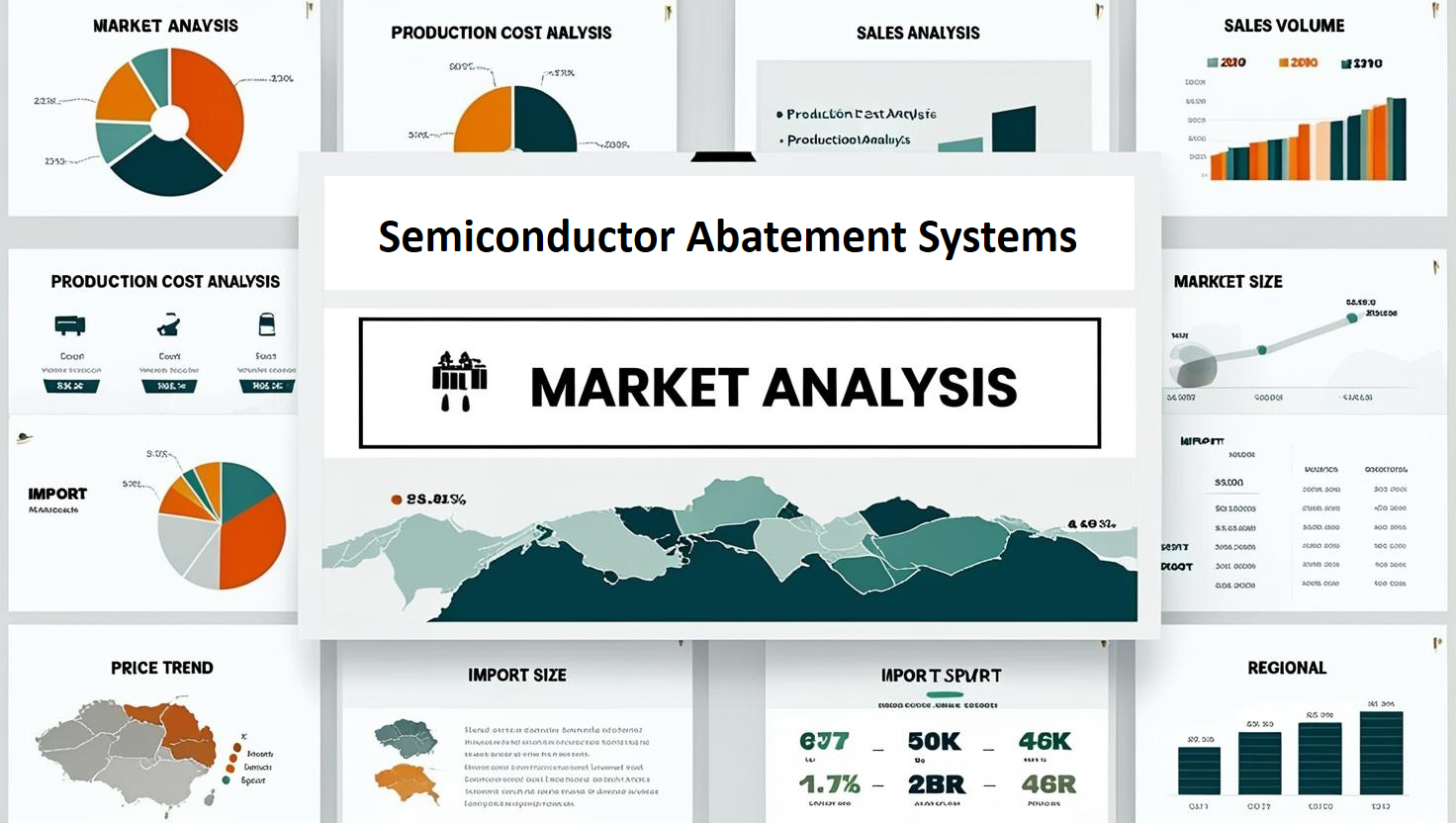
Semiconductor Abatement Systems Market Momentum and the 2026 Outlook
According to Staticker, the Semiconductor Abatement Systems market size in 2026 is expected to reflect strong expansion driven by new fabrication investments, advanced packaging capacity additions, and increasingly stringent emissions management requirements across major chip-producing regions. Staticker projects sustained growth for the Semiconductor Abatement Systems market through the forecast period as manufacturers prioritize greenhouse-gas reduction, facility permitting compliance, and integrated sustainability infrastructure. The growth trajectory is being reinforced by the construction of new fabs, rising utilization of advanced process gases, and higher adoption rates of point-of-use Semiconductor Abatement Systems in both logic and memory manufacturing environments.
Mapping the Major Use Cases Across the Fab
The first major use case for Semiconductor Abatement Systems occurs in plasma etching.
Plasma etching can account for a significant share of greenhouse-gas-related process emissions. Because advanced chips require hundreds of precise etch operations, emissions treatment infrastructure must scale proportionally. Semiconductor Abatement Systems installed near etch tools minimize transport distance and improve treatment effectiveness.
The second use case is chemical vapor deposition.
Deposition chambers create thin material layers measured in nanometers. Although these layers are microscopic, the supporting chemical processes generate exhaust streams requiring continuous treatment. Semiconductor Abatement Systems ensure that deposition throughput can increase without creating corresponding environmental burdens.
The third use case involves advanced packaging facilities.
Packaging has become a strategic industry segment due to AI accelerators, high-bandwidth memory, and chiplet architectures. Advanced packaging plants often incorporate specialized cleaning, bonding, and material deposition processes. As these facilities expand, Semiconductor Abatement Systems are increasingly deployed beyond traditional front-end wafer fabs.
The fourth use case is research and pilot production.
Research facilities may operate fewer tools, but they frequently test new chemistries. Semiconductor Abatement Systems provide flexibility for handling changing process conditions while maintaining environmental compliance.
The Economics Behind Adoption
The financial logic supporting Semiconductor Abatement Systems extends beyond regulation.
A semiconductor fabrication facility can represent investments exceeding several billion dollars. Delays related to permitting, environmental compliance, or emissions management can affect production schedules and return on capital.
Consequently, Semiconductor Abatement Systems function as risk-reduction assets. Their value is measured not only through emissions reduction but also through uninterrupted manufacturing operations.
Many facilities evaluate performance using metrics such as treatment efficiency, energy consumption per treated volume, uptime percentage, maintenance intervals, and total cost of ownership. Improvements in these metrics can create operational savings over equipment lifecycles that often exceed 10 years.
As semiconductor production expands globally, Semiconductor Abatement Systems are becoming a strategic infrastructure category that supports manufacturing growth, sustainability commitments, and long-term industrial competitiveness simultaneously.
Request for customization: https://staticker.com/reports/semiconductor-abatement-systems-market/
Categorias
Leia mais
If you are searching for Burn Slim supplement real results after 30 days, you are likely looking for an honest breakdown of whether this trending weight loss formula truly helps with fat burning, metabolism support, and appetite control. Many people in the USA are talking about Burn Slim because it is marketed as a natural metabolism booster supplement designed to support weight management,...

The modern marketplace is overflowing with groundbreaking ideas, aggressive competitors, and companies racing to dominate entire industries overnight. In this relentless environment, protecting a product’s visual uniqueness has become a mission-critical priority. This is exactly why professional design patent drawings have emerged as one of the most valuable assets for inventors and...
Nokia has always been one of the most trusted mobile phone brands in Pakistan due to its durability, strong battery life, and simple user experience. Even in today’s modern smartphone era, Nokia continues to maintain its identity by launching budget-friendly and mid-range smartphones that meet the needs of everyday users. Many people still search for Nokia Mobile Price in Pakistan because...

"U.K. Radiology Services Market Summary: According to the latest report published by Data Bridge Market Research, the U.K. Radiology Services Market CAGR Value Data Bridge Market Research analyses that the U.K. radiology services market which was USD 13.94 billion in 2022, is expected to reach USD 23.84 billion by 2030, and is expected to undergo a CAGR of 17.2% during the forecast...
Why Choosing the Right Tools Matters Before we look at the list, it is important to understand why tool selection is important. A good cutting setup improves surface finish, reduces machine load, and increases tool life. On the other hand, using the wrong option can lead to poor results, tool breakage, and wasted material. Also, many people now prefer buying from a cnc tool online shop india...