


How 3D Integrated Circuits (3D ICs) Are Rewriting the Economics of AI, Data Centers, and Advanced Computing Infrastructure
How 3D Integrated Circuits (3D ICs) Are Rewriting the Economics of AI, Data Centers, and Advanced Computing Infrastructure
The semiconductor industry has entered an era where shrinking transistors is no longer the only path to performance. The next leap is vertical. The story of 3D Integrated Circuits (3D ICs) market is not merely about stacking chips; it is about redesigning the physical architecture of computation itself.
For nearly five decades, semiconductor progress followed a horizontal roadmap. More transistors were packed into smaller areas, enabling higher performance generation after generation. However, as process nodes moved below 10 nanometers, the cost of scaling began rising faster than the performance benefits. In several advanced manufacturing facilities, wafer fabrication investments now exceed billions of dollars per production line, forcing the industry to seek alternatives.
This is where 3D Integrated Circuits (3D ICs) emerged as a strategic infrastructure solution.
Instead of placing processors, memory, accelerators, and communication components side by side, 3D Integrated Circuits (3D ICs) stack them vertically using through-silicon vias, hybrid bonding, and advanced packaging technologies. The result is shorter communication pathways, lower latency, higher bandwidth, and significantly improved performance per watt.
The impact becomes visible when examining data movement. In modern AI systems, more than 60% of total energy consumption can be associated with moving data between memory and compute resources rather than performing calculations themselves. By reducing interconnect distances from centimeters to micrometers, 3D Integrated Circuits (3D ICs) can dramatically improve energy efficiency while increasing computational throughput.
The Infrastructure Story: Building Up Instead of Out
Every technological revolution is fundamentally an infrastructure story.
Cloud computing required hyperscale data centers.
5G required dense antenna networks.
Artificial intelligence requires a new computing architecture.
That architecture increasingly points toward 3D Integrated Circuits (3D ICs).
Consider a conventional processor package. Signals often travel several millimeters or even centimeters between compute and memory components. In advanced stacked architectures, those distances shrink by factors of hundreds or thousands. Electrical resistance decreases, signal integrity improves, and bandwidth expands.
A modern high-bandwidth memory stack can deliver data transfer rates exceeding several terabytes per second. Such performance would be difficult to achieve economically through traditional planar architectures.
The infrastructure supporting 3D Integrated Circuits (3D ICs) extends far beyond semiconductor fabs. It includes advanced packaging facilities, wafer bonding systems, precision metrology tools, thermal management platforms, and automated inspection equipment.
Industry investments increasingly reflect this shift. Advanced packaging capacity expansions have become a strategic priority across major semiconductor manufacturing regions including North America, East Asia, and Europe. In many cases, packaging investment growth rates are outpacing traditional front-end wafer fabrication expansion because packaging has become a performance differentiator rather than a finishing step.
Why AI Became the Catalyst for 3D Integrated Circuits (3D ICs)
Artificial intelligence is fundamentally a bandwidth problem.
Training large language models requires moving enormous datasets across processors, memory subsystems, networking infrastructure, and storage arrays. A single AI training cluster may contain tens of thousands of accelerators connected through high-speed interconnects.
In such environments, every nanosecond matters.
This is why 3D Integrated Circuits (3D ICs) have become central to AI hardware design. Stacked memory architectures enable significantly faster data access compared with traditional memory configurations. Reduced communication distances also lower power consumption, a critical metric as AI facilities increasingly face energy constraints.
A large AI data center can consume hundreds of megawatts of power. Even a 10% improvement in compute efficiency can translate into substantial operational savings over the facility lifecycle.
The economics are straightforward.
When compute demand grows by multiples, infrastructure operators cannot simply scale energy consumption at the same rate. They need architectural innovations. 3D Integrated Circuits (3D ICs) provide one of the most effective pathways toward that objective.
Market Momentum Signals a Structural Shift
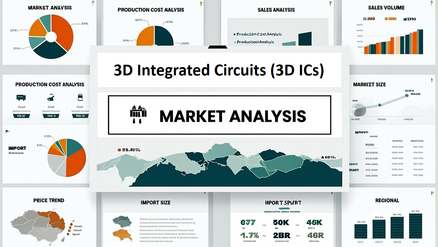
According to Staticker, the global 3D Integrated Circuits (3D ICs) market in 2026 is expected to demonstrate strong year-on-year expansion, with sustained double-digit growth projected through the forecast period as AI accelerators, high-performance computing systems, advanced memory architectures, automotive electronics, and edge computing deployments continue increasing demand for vertically integrated semiconductor designs. The forecast suggests that adoption rates for 3D Integrated Circuits (3D ICs) will outpace many conventional semiconductor packaging approaches as manufacturers prioritize performance-per-watt improvements, bandwidth density, and heterogeneous integration strategies across next-generation computing platforms.
Mapping the Use Cases: Where Vertical Integration Changes Everything
The first major application area for 3D Integrated Circuits (3D ICs) is high-performance computing.
Supercomputers increasingly require dense computational architectures capable of processing trillions of operations per second. In these systems, reducing communication bottlenecks often delivers greater performance gains than simply adding more cores.
A second major application is AI inference.
As enterprises deploy generative AI into customer service, software development, healthcare analytics, and industrial automation, inference workloads are becoming larger and more frequent. Low-latency memory access enabled by 3D Integrated Circuits (3D ICs) helps accelerate these deployments while maintaining energy efficiency.
A third use case is automotive electronics.
Modern vehicles increasingly resemble data centers on wheels. Advanced driver-assistance systems process inputs from cameras, radar, lidar, and numerous sensors simultaneously. Some premium vehicles generate multiple terabytes of data daily during operation and testing.
To process such information efficiently, automotive chip designers are adopting architectures associated with 3D Integrated Circuits (3D ICs). The benefits include smaller footprints, faster processing, and improved reliability under constrained space conditions.
The fourth use case is edge computing.
Factories, logistics hubs, hospitals, and telecommunications facilities increasingly require local processing capabilities. Sending every workload to centralized cloud infrastructure introduces latency and bandwidth costs.
Compact systems based on 3D Integrated Circuits (3D ICs) allow edge devices to deliver greater computational density within limited physical space, making them attractive for distributed infrastructure deployments.
The Thermal Challenge That Created an Engineering Race
Every technological breakthrough creates a new bottleneck.
For 3D Integrated Circuits (3D ICs), that bottleneck is heat.
Stacking silicon layers improves performance but also increases thermal density. Engineers must now manage heat flow through multiple semiconductor layers rather than a single surface.
The numbers are significant. Power densities in advanced AI processors continue rising, requiring innovative cooling architectures. This has triggered substantial investment into liquid cooling systems, thermal interface materials, microfluidic technologies, and advanced heat spreaders.
As a result, the growth of 3D Integrated Circuits (3D ICs) is also stimulating adjacent infrastructure sectors including cooling equipment, advanced materials, semiconductor packaging tools, and precision manufacturing technologies.
The story therefore extends beyond semiconductors. It is becoming a broader industrial ecosystem transformation where computing, manufacturing, energy efficiency, and materials science converge around a common objective: extracting more performance from every square millimeter of silicon.
Request for customization: https://staticker.com/reports/3d-integrated-circuits-3d-ics-market/
Κατηγορίες
Διαβάζω περισσότερα
온라인 배팅 시장이 급격히 팽창하면서 사용자들은 수많은 플랫폼 중에서 어디를 선택해야 할지 고민에 빠지게 됩니다. 하지만 화려한 인터페이스와 높은 배당률 뒤에는 항상 자금 탈취의 위험이 도사리고 있습니다. 이러한 위험을 사전에 차단하고 내 자산을 지키기 위해서는 신뢰할 수 있는 커뮤니티의 도움을 받는 것이 가장 현명한 방법입니다. 먹튀검증 시스템의 체계적 이해 단순히 사이트의 외형만 보고 안전을 판단하는 시대는 지났습니다. 진정한 안전을 확보하기 위해서는 해당 플랫폼의 운영 기간, 서버 보안 상태, 그리고 과거의 사고 이력까지 낱낱이 파헤쳐야 합니다. 먹튀런은 이러한 복잡한 과정을 대신 수행하여 사용자들에게 투명한 정보를 제공함으로써 건전한 스포츠 배팅 환경을 구축하는 데 기여하고 있습니다. 먹튀...

BloodArmor ⇨Claim Now₰₰ https://alltopsupplement.com/BloodArmor BloodArmor is a dietary supplement designed to support healthy blood sugar levels and insulin sensitivity. It typically features natural ingredients like Cinnamon, Chromium, and Berberine. While it may offer mild metabolic support, it is not a replacement for prescribed medications and should be discussed with a doctor before use....
Football is not just a sport; it is a global passion that connects millions of fans across continents. In today’s fast-paced digital world, fans no longer wait for television highlights or next-day newspapers to know what happened in a match. Instead, they rely on instant updates, live statistics, and real-time score tracking platforms. This is where modern digital...
How New Users Can Get Started on Sky Exchange Without Any Confusion The world of online gaming and betting can seem complicated for beginners. With so many platforms available, new users often feel confused about where to start, how to create an account, and what features they should use first. Sky Exchange has become a popular choice because it offers a simple, user-friendly...
Market Overview Global Electric Ship Pod Drives Market size and share is currently valued at USD 1,006.31 million in 2024 and is anticipated to generate an estimated revenue of USD 2,150.20 Million by 2034, according to the latest study by Polaris Market Research. Besides, the report notes that the market exhibits a robust 7.9% Compound Annual Growth Rate (CAGR) over the forecasted...