


Wafer Level Low-Loss Materials: The Invisible Infrastructure Powering the Next Trillion Connected Devices
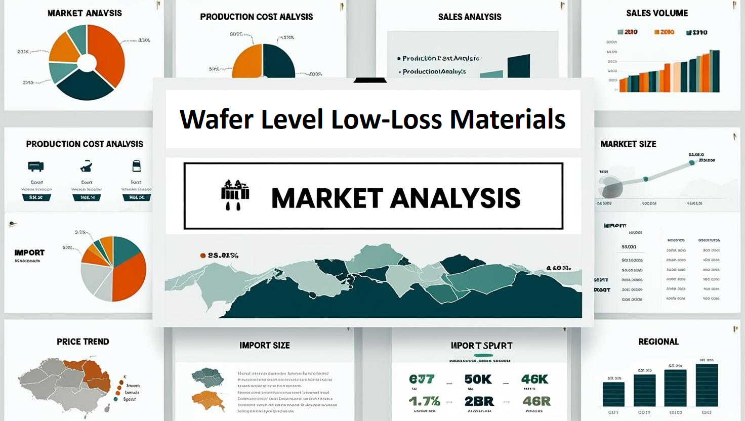
Wafer Level Low-Loss Materials: The Invisible Infrastructure Powering the Next Trillion Connected Devices
Every technology cycle has a hidden layer that determines whether innovation scales or stalls. In the age of 5G Advanced, AI-enabled edge computing, satellite broadband, autonomous systems, and high-frequency sensing, that hidden layer is increasingly built around Wafer Level Low-Loss Materials market.
The semiconductor industry often celebrates processors, memory, and advanced packaging. Yet as signal frequencies move from traditional sub-6 GHz communications toward 28 GHz, 39 GHz, 77 GHz, 110 GHz and beyond, electrical losses become a critical engineering challenge. A signal losing even 1–2 dB of performance across multiple pathways can reduce communication efficiency by more than 20%, forcing designers to compensate through higher power consumption, larger antennas, or more expensive architectures.
This is where Wafer Level Low-Loss Materials emerge as a foundational infrastructure theme. They are not merely specialty materials. They are becoming performance multipliers across telecommunications, automotive electronics, aerospace systems, AI hardware, and advanced consumer devices.
Industry estimates indicate that more than 65% of advanced RF package development programs initiated after 2023 include evaluation of new Wafer Level Low-Loss Materials during the design phase. The reason is straightforward: every gigahertz increase in operating frequency amplifies the importance of dielectric performance, insertion loss control, and signal integrity.
The Infrastructure Behind High-Frequency Computing
Modern semiconductor infrastructure is no longer limited to transistor scaling. It now includes packaging ecosystems, substrate engineering, wafer-level integration facilities, and material science laboratories.
A typical advanced semiconductor manufacturing cluster may invest 15–25% of its packaging development budget into material characterization and reliability testing. Within that allocation, Wafer Level Low-Loss Materials represent one of the fastest-growing categories because they directly influence electrical performance.
Consider a high-frequency communication module operating at 77 GHz for automotive radar. Traditional materials can introduce dielectric losses that reduce detection precision over long distances. By deploying optimized Wafer Level Low-Loss Materials, manufacturers can improve signal transmission efficiency by 10–30%, depending on architecture and frequency range.
This improvement creates cascading benefits:
-
Higher sensing accuracy
-
Lower power consumption
-
Reduced thermal generation
-
Longer operating life
-
Smaller package footprints
The infrastructure requirement extends beyond material production. It includes deposition systems, wafer bonding equipment, metrology tools, dielectric testing platforms, reliability chambers, and advanced simulation environments.
A modern wafer-level packaging facility may process hundreds of thousands of wafers annually, and even a 1% improvement in signal efficiency can translate into millions of dollars in operational value across production volumes.
Why Frequency Growth Is Creating a New Materials Economy
The global electronics ecosystem is experiencing a frequency migration.
4G infrastructure primarily operated below 6 GHz. Modern wireless systems increasingly utilize millimeter-wave frequencies. Automotive radar has shifted toward 77 GHz standards. Satellite communication networks routinely utilize Ka-band frequencies exceeding 26 GHz.
At these frequencies, material behavior changes dramatically.
Electrical energy interacting with substrates encounters dielectric losses that can degrade performance. Consequently, Wafer Level Low-Loss Materials have become essential engineering components rather than optional enhancements.
A useful comparison can be made with transportation infrastructure.
If data signals are vehicles, then semiconductor interconnects are highways. Traditional materials resemble roads with increasing friction. Wafer Level Low-Loss Materials effectively reduce that friction, allowing more information to travel with less energy loss.
For large-scale network deployments, even a 5% reduction in transmission losses can generate substantial efficiency gains. Across millions of devices, this translates into lower energy requirements, improved battery life, and enhanced network performance.
Market Momentum Signals a Structural Shift
According to Staticker, the Wafer Level Low-Loss Materials market in 2026 is expected to demonstrate strong year-over-year expansion, supported by accelerating deployment of advanced packaging technologies, RF front-end modules, automotive radar systems, satellite communication hardware, and AI-enabled edge devices. Staticker projects sustained double-digit growth momentum through the forecast period as semiconductor manufacturers increase investments in wafer-level packaging infrastructure and next-generation communication architectures. The growth trajectory of Wafer Level Low-Loss Materials is being reinforced by rising frequency requirements, increasing signal-integrity demands, and greater adoption of heterogeneous integration strategies across multiple electronics sectors.
Mapping the Most Important Use Cases
The first major application category for Wafer Level Low-Loss Materials is telecommunications infrastructure.
A single 5G base station can process enormous data volumes every day while operating across multiple frequency bands. Signal degradation directly impacts coverage quality and network efficiency. By incorporating Wafer Level Low-Loss Materials, equipment manufacturers can reduce insertion losses and improve radio performance without proportionally increasing power requirements.
The second major use case is automotive radar.
Modern vehicles increasingly incorporate radar sensors for adaptive cruise control, collision avoidance, lane monitoring, and autonomous driving functions. Premium vehicles may contain between 5 and 15 radar units.
As radar resolution requirements increase, manufacturers require Wafer Level Low-Loss Materials capable of maintaining stable electrical properties under temperature variations ranging from -40°C to +125°C.
Even a modest 10% improvement in signal quality can enhance object detection reliability, especially under challenging environmental conditions.
The third application category is satellite communications.
Low Earth Orbit constellations are expanding rapidly. Each satellite contains communication modules operating under strict power constraints. Every watt saved contributes directly to mission efficiency.
For this reason, aerospace manufacturers increasingly evaluate Wafer Level Low-Loss Materials capable of reducing transmission losses while maintaining radiation tolerance and long-term reliability.
The AI Hardware Connection
Artificial intelligence infrastructure is creating another major growth pathway.
While most AI discussions focus on processors and GPUs, the movement of data between components increasingly determines system efficiency. High-bandwidth communication links require materials capable of preserving signal integrity at ever-increasing speeds.
Advanced packaging architectures are therefore integrating Wafer Level Low-Loss Materials into interconnect structures, redistribution layers, and high-frequency communication pathways.
In large AI computing environments, even small reductions in transmission losses can compound across thousands of interconnected processors.
A 2–3% improvement in communication efficiency may appear minor at the component level. Across hyperscale infrastructure, however, those gains can translate into significant reductions in power consumption, cooling requirements, and operating expenses.
The result is a new engineering reality: material science is becoming as strategically important as chip design itself. As frequency requirements continue to rise and device architectures become increasingly complex, Wafer Level Low-Loss Materials are evolving from a specialized packaging consideration into a core enabling technology for the digital infrastructure economy.
Request for customization: https://staticker.com/reports/wafer-level-low-loss-materials-market/
Categorias
Leia mais
Milliseconds now determine competitive advantage. Autonomous vehicles cannot wait for cloud processing. Smart grids cannot pause during outages. Industrial robots cannot tolerate lag. This is why leading organizations are partnering with an advanced IoT App Development Company to implement edge AI architectures that deliver instantaneous insights. What Is Edge Intelligence in IoT? Edge...

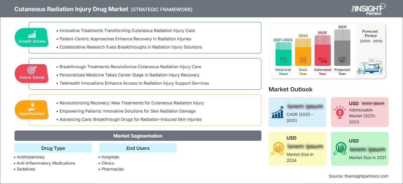
The cutaneous radiation injury (CRI) drug market is expected to grow significantly by 2031, driven by the increasing use of radiation therapy in cancer treatment, rising awareness of radiation-related skin injuries, and advances in pharmaceutical therapies. cutaneous radiation injury (CRI) drug market Segmentation Analysis reveals that the industry is categorized by drug type, end user, and...
Retaining wall design is an important part of structural engineering, especially in projects where there is a difference in ground levels. Retaining walls are used to hold back soil and prevent it from sliding or collapsing due to gravity. These structures are commonly used in basements, hillside buildings, road construction, landscaping, and infrastructure projects. A properly designed...

In heavy industries, equipment either performs or it becomes a problem. There’s rarely anything in between. And when it comes to heat exchangers, companies don’t have time for constant maintenance headaches, leaks, or systems that struggle under pressure. That’s one reason why jatco shell and tube systems keep getting picked across different sectors, from petrochemical...
It is important for any business that wants success in today’s online environment to have an effective SEO strategy aimed at boosting its visibility, attracting targeted clients, and improving its overall authority. One way of achieving these goals is guest post link building which is very efficient in terms of acquiring top-quality backlinks that result in high rankings. Why Guest...