PCB Design Software Market Analysis of CAGR and Emerging Trends: Competitive Landscape to US$ 11.2 Million
PCB design software often includes 3D visualization and mechanical integration features. Designers can view the board in a realistic environment, check component fit, and avoid mechanical conflicts before production. This improves collaboration between electronic and mechanical design teams and reduces costly revisions.
Market Overview
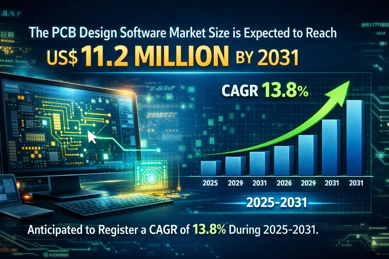
The PCB Design Software Market is poised for substantial expansion, with projections indicating that the market size will reach US$ 11.2 million by 2031, registering a CAGR of 13.8% during the forecast period from 2025 to 2031. Printed circuit board design software plays a critical role in modern electronics development by enabling engineers to design, simulate, and validate complex circuit layouts before production. As industries accelerate digital transformation and product innovation cycles shorten, demand for advanced design tools continues to rise.
The report by The Insight Partners provides a comprehensive analysis of current market conditions, emerging trends, and growth prospects across global, regional, and country levels. Historical data from 2021 to 2023 forms the basis for future projections, ensuring robust financial modeling and strategic forecasting.
Segmentation Analysis: PCB Design Software Market by Complexity and Industry Vertical
The PCB Design Software Market is segmented by complexity into high-end, medium-end, and low-end solutions. High-end software caters to advanced industries such as aerospace and semiconductor manufacturing, where multi-layer boards and high-frequency designs are common. These tools offer advanced simulation, signal integrity analysis, and integration capabilities. Medium-end solutions serve mid-sized enterprises and growing technology firms seeking efficiency and moderate design complexity. Low-end solutions are typically adopted by startups, educational institutions, and small-scale electronics manufacturers due to affordability and ease of use.
From an industry vertical perspective, the market spans aerospace and defense, consumer electronics, education and research, healthcare, semiconductors, telecommunication, and transportation. The aerospace and defense segment demands highly reliable and precision-driven tools to meet regulatory and safety standards. Consumer electronics remains a major revenue contributor due to the proliferation of smart devices and IoT products. Healthcare applications, including medical devices and diagnostic equipment, require compact and highly reliable PCB architectures. Meanwhile, the semiconductor and telecommunication sectors drive demand for high-speed and high-frequency design capabilities.
Download Sample PDF:https://www.theinsightpartners.com/sample/TIPTE00002170
Growth Drivers
Several factors are fueling growth across the PCB Design Software Market. Increasing complexity in electronic devices is pushing manufacturers to adopt sophisticated design environments capable of managing multilayer boards and miniaturized components. Automation within design workflows is improving accuracy and reducing time to market. Integration with manufacturing systems streamlines production cycles and minimizes costly errors.
The push toward innovation across sectors such as automotive electrification and 5G infrastructure is also stimulating demand. User-centric interfaces and intuitive design platforms are lowering entry barriers for startups and small enterprises, further broadening the customer base. Additionally, cloud-based deployment models are enhancing collaboration and scalability across distributed engineering teams.
Emerging Trends and Market Opportunities
Artificial intelligence is becoming a transformative force within the PCB Design Software Market. AI-powered layout optimization, predictive error detection, and automated routing are revolutionizing electronics development. These capabilities enable faster prototyping and reduce design iterations.
Sustainability is another prominent trend. Software tools are increasingly incorporating eco-friendly material selection guidelines and energy-efficient design optimization features. As regulatory scrutiny intensifies, sustainable PCB development practices are becoming a competitive differentiator.
Collaborative cloud platforms represent another significant opportunity. Real-time co-design environments bridge geographically dispersed teams, improving communication and reducing project delays. Such platforms are particularly beneficial for multinational enterprises operating across North America, Europe, and Asia-Pacific.
Regional Insights Across the PCB Design Software Market
North America holds a significant share of the PCB Design Software Market, supported by strong semiconductor and aerospace industries in the US and Canada. Europe follows closely, with innovation hubs in the UK, Germany, and France contributing to technological advancements. Asia-Pacific is expected to witness the fastest growth, driven by electronics manufacturing powerhouses such as China, Japan, and India. Expanding consumer electronics production and government support for semiconductor fabrication strengthen the regional outlook.
Emerging economies in South and Central America and the Middle East and Africa are gradually increasing adoption rates as digital infrastructure expands and industrial automation gains traction.
Key Players
Leading companies are investing in research and development, strategic collaborations, and product innovation to maintain competitive advantage.
-
Altium Limited
-
Autodesk Inc.
-
ANSYS, Inc.
-
Cadence Design Systems, Inc.
-
Dassault Systèmes
-
Novarm Limited
-
Siemens
-
Synopsys, Inc.
-
Westdev
-
Zuken
These players are focusing on AI integration, cloud deployment models, and cross-platform compatibility to enhance user experience and strengthen market positioning.
Future Outlook
The future of the PCB Design Software Market appears promising as digitalization accelerates across industries. The convergence of AI, cloud computing, and sustainable engineering practices will redefine design methodologies. Growing investments in semiconductor manufacturing, electric vehicles, and next-generation communication networks will further elevate demand. As innovation cycles shorten and product complexity rises, advanced PCB design tools will become indispensable. Companies that prioritize automation, collaboration, and sustainability will likely lead the next phase of market evolution through 2031.
Related Reports:
Κατηγορίες
Διαβάζω περισσότερα
Introduction The future of recovery lies in natural, plant-based solutions. Among these, terpology recovery terpenes stand out as a key innovation. These compounds enhance the benefits of medical cannabis and help patients manage complex conditions. Evergreen Terpene provides legal access to these solutions across the UK, ensuring patients receive safe and reliable care. What Makes Terpenes...

Market Overview According To The Research Report Published By Polaris Market Research, The Global Military Antennas Market Was Valued At Usd 3.97 Billion In 2021 And Is Expected To Reach Usd 6.33 Billion By 2030, To Grow At A Cagr Of 5.7% During The Forecast Period. The global Military Antennas Market is witnessing significant growth due to the rising demand for advanced communication...

In recent years, online gaming and sports betting platforms have gained huge popularity in India. One such name that’s frequently talked about is SkyExchange 247. Whether you’re a cricket fan, casino lover, or someone curious about online betting platforms, this guide will help you understand everything in a simple and clear way. What is SkyExchange 247? SkyExchange 247 is...
"Executive Summary Cholera Treatment Market: Share, Size & Strategic Insights The global cholera treatment market size was valued at USD 149.36 million in 2024 and is projected to reach USD 278.51 million by 2032, with a CAGR of 8.10% during the forecast period of 2025 to 2032. The Cholera Treatment report provides CAGR values along with its fluctuations for the specific forecast...
Greetings from Bangalore, the capital of the state of Karnataka. You've come to the perfect place if you're seeking some fascinating company while you're in Bangalore or are planning a trip to this lovely hill city. Welcome to our call girl in Bangalore, where we pair you with the most attractive and seductive people in the area. We have everything you need, whether you're looking for...