Global Semiconductor Defect Inspection System Industry Trends and Key Growth Drivers Toward 2034
The semiconductor industry continues to evolve rapidly as manufacturers develop increasingly advanced integrated circuits to support emerging technologies such as artificial intelligence, high-performance computing, 5G connectivity, and intelligent consumer electronics. Semiconductor fabrication processes involve extremely precise manufacturing stages where even the smallest defect at the microscopic level can impact chip performance, reliability, and overall production yield. As chip designs become more complex and process nodes shrink further, maintaining strict quality control across semiconductor production has become a critical priority for manufacturers worldwide.
To address these challenges, advanced inspection technologies are widely deployed across semiconductor fabrication facilities. These systems are designed to identify microscopic defects, contamination, and structural irregularities during wafer processing. By integrating optical inspection, electron beam imaging, and advanced analytics, manufacturers can monitor semiconductor production in real time and detect issues before they affect large-scale wafer batches. The increasing complexity of semiconductor architectures and advanced packaging technologies is making defect inspection systems an essential part of modern semiconductor manufacturing environments.
The Semiconductor Defect Inspection System Market is experiencing strong global growth as semiconductor manufacturers increase investments in advanced fabrication technologies and quality assurance solutions. The Semiconductor Defect Inspection System Market Analysis is expanding as demand rises for high-performance semiconductor devices used in artificial intelligence, data centers, automotive electronics, telecommunications infrastructure, and consumer electronics. Continuous advancements in semiconductor process technologies, combined with increasing investments in fabrication facilities, are further accelerating the adoption of advanced inspection systems across global semiconductor manufacturing ecosystems.
Download Sample PDF Copy of this Report:
https://www.theinsightpartners.com/sample/TIPRE00017006
Rising Global Demand for Semiconductor Devices
One of the most significant drivers supporting the expansion of semiconductor defect inspection technologies is the increasing global demand for semiconductor devices. Industries such as consumer electronics, automotive, healthcare, industrial automation, and telecommunications rely heavily on semiconductor components for advanced digital operations.
As electronic devices become more powerful and compact, semiconductor manufacturers must ensure that production processes maintain extremely high levels of precision. Defect inspection systems allow manufacturers to detect microscopic wafer imperfections early in the fabrication process, preventing defective chips from progressing through production lines. This capability significantly improves manufacturing yield and reduces costly production losses.
Miniaturization of Semiconductor Process Nodes
The semiconductor industry continues to advance toward smaller process nodes in order to improve device performance, increase processing speed, and reduce power consumption. However, the transition to smaller geometries significantly increases the complexity of semiconductor manufacturing processes.
At nanometer-scale dimensions, even the smallest particle contamination or structural irregularity can impact chip functionality. Advanced semiconductor defect inspection systems provide ultra-high-resolution imaging technologies that enable engineers to detect nanoscale defects during wafer fabrication. As semiconductor devices continue to shrink in size, the need for highly sophisticated inspection technologies is expected to grow significantly.
Increasing Complexity of Semiconductor Fabrication Processes
Modern semiconductor manufacturing involves hundreds of precise process steps, including lithography, deposition, etching, cleaning, and advanced packaging. Each stage introduces potential defects that could affect chip functionality and production yield.
Defect inspection systems help monitor wafer quality throughout these complex production stages. By detecting process variations and structural defects early, manufacturers can optimize fabrication workflows and maintain consistent production performance. These systems therefore play a crucial role in process control, yield management, and quality assurance across semiconductor manufacturing facilities.
Growth of Artificial Intelligence and High-Performance Computing
The rapid expansion of artificial intelligence, machine learning, and high-performance computing applications is significantly increasing demand for advanced semiconductor processors. AI workloads require powerful chips capable of processing massive volumes of data at high speeds.
To produce these sophisticated processors, semiconductor manufacturers must maintain extremely high production accuracy. Semiconductor defect inspection systems allow engineers to identify potential manufacturing defects that could affect chip performance. As global investments in AI technologies and data center infrastructure continue to rise, the demand for advanced inspection technologies is expected to grow further.
Technological Advancements in Inspection Solutions
Technological innovation is continuously improving the performance and efficiency of semiconductor defect inspection systems. Modern inspection platforms integrate high-speed optical scanning technologies, electron beam imaging, and artificial intelligence-driven analytics to enhance defect detection accuracy.
Machine learning algorithms are increasingly being used to analyze inspection data, classify defects, and identify recurring manufacturing issues. These intelligent systems help semiconductor manufacturers improve process control, reduce production downtime, and enhance operational efficiency.
Automation and real-time monitoring capabilities are also enabling semiconductor fabrication facilities to implement advanced process management strategies and predictive maintenance programs.
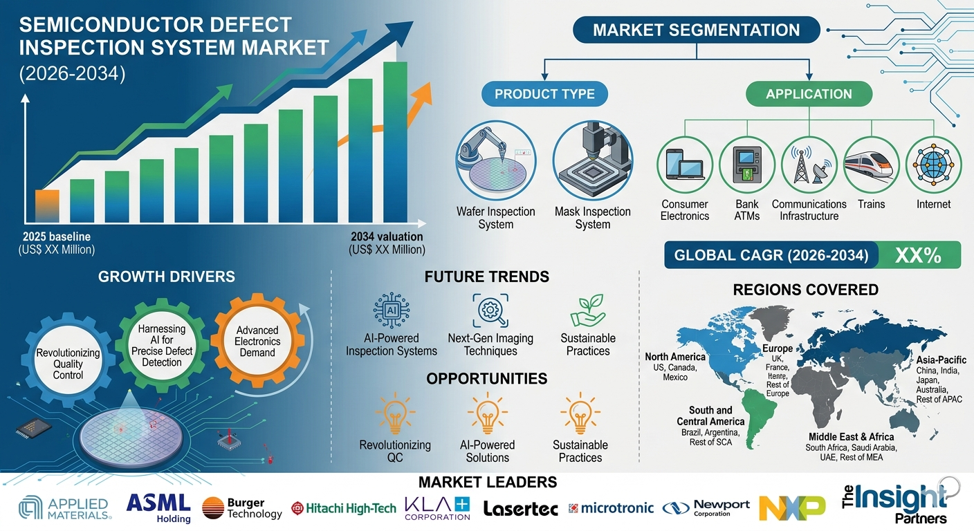
Competitive Landscape and Key Players
The semiconductor defect inspection system industry is highly competitive, with several global technology companies specializing in semiconductor manufacturing equipment and process control technologies. These companies continue to invest heavily in research and development to enhance inspection capabilities and support next-generation semiconductor fabrication processes.
Key companies operating in the industry include:
KLA Corporation
Applied Materials Inc.
ASML Holding N.V.
Hitachi High-Tech Corporation
Onto Innovation Inc.
Camtek Ltd.
Lasertec Corporation
SCREEN Semiconductor Solutions
Advantest Corporation
Toray Engineering Co., Ltd.
These companies are focusing on developing advanced inspection technologies capable of detecting increasingly complex defects while improving wafer yield and manufacturing efficiency.
Future Outlook
The global semiconductor defect inspection system industry is expected to witness significant growth through 2034 as semiconductor manufacturing continues to expand across multiple industries. Increasing demand for high-performance chips, rapid advancements in artificial intelligence technologies, and the growing complexity of semiconductor fabrication processes will continue to support industry expansion.
Emerging innovations in artificial intelligence-driven inspection systems, high-resolution imaging technologies, and automated process monitoring platforms will further enhance defect detection capabilities. As semiconductor manufacturing technologies continue to evolve, defect inspection systems will remain essential for maintaining product quality, improving production efficiency, and supporting the development of next-generation semiconductor devices.
About Us
The Insight Partners is a global market research and consulting firm delivering comprehensive industry insights and strategic intelligence across multiple sectors. Our research reports provide in-depth analysis of industry trends, technological developments, competitive landscapes, and growth opportunities, helping organizations make informed business decisions and achieve sustainable growth.
Contact Us
The Insight Partners
Email: sales@theinsightpartners.com
Phone: +1-646-491-9876
Website: https://www.theinsightpartners.com
Related Reports -
Embedded Computing Market Share, Trends, and Growth Opportunity
Digital Twin Technology MarketShare, Trends, and Growth Opportunity
Categorie
Leggi tutto
Creating a safe learning environment is essential for every educational institution, and one of the most effective ways to achieve this is through well-trained safety officers. Modern campuses face a wide range of security challenges, from theft and vandalism to more serious threats involving violence or unauthorized intrusions. In the first line of defense, teams such as University Security...

In today’s competitive digital space, users are constantly searching for platforms that offer reliability, speed, and a smooth experience. Mahadev Book has emerged as a popular choice among thousands of users due to its user-friendly design and efficient features. Whether it’s easy access through Mahadev Book Login or seamless usage via the Mahadev Book App,...
Prepare confidently with DumpsHero’s updated FSCP Dumps and verified FSCP PDF Dumps. Get accurate, exam-focused study guides designed to help you pass the Forescout FSCP certification exam successfully on your first try. FSCP Exam Dumps to Achieve Excellent Results on Your First Attempt DumpsHero provides highly dependable Forescout FSCP exam dumps designed to support your...
La marcatura laser metalli rappresenta oggi uno dei metodi più avanzati per incidere, identificare e personalizzare superfici metalliche con estrema precisione. In numerosi settori industriali, la richiesta di marcature permanenti, leggibili e professionali è diventata fondamentale. Per questo motivo, molte aziende stanno adottando sistemi laser per realizzare codici, numeri...

Starting your own short video sharing app using a TikTok clone script is never too late, particularly in the Western market. Everyone believes the short-form video market is already dominated. TikTok is the king. Instagram Reels and YouTube Shorts are just playing catch-up. But that's looking at the wrong window. The short video platform industry is set to go beyond $3B by 2030, but the smart...